SOCAMM2 Explained: The 694-Pin LPDDR Module Reshaping AI Server Memory in 2026
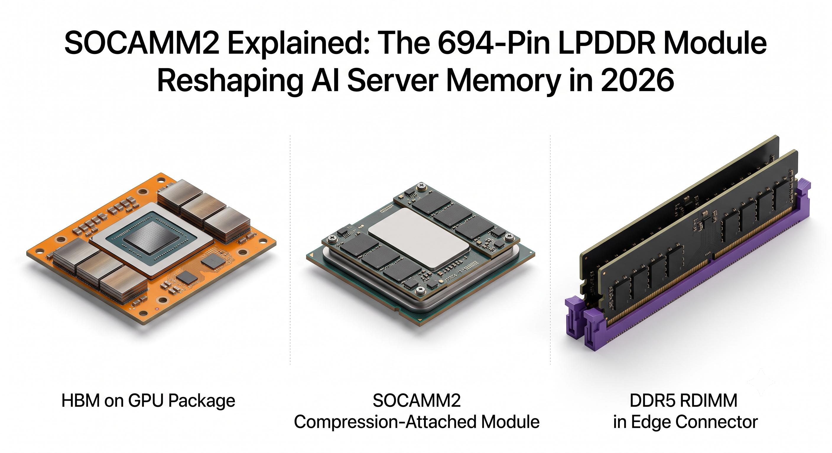
SOCAMM2 is a JEDEC-standardized, compression-attached LPDDR5X memory module that sits next to the CPU in an AI server — it is not an HBM competitor and never was. HBM lives on the GPU package and answers a bandwidth question; SOCAMM2 goes into the socket-adjacent slot that DDR5 RDIMM used to own and answers a capacity-per-watt question. The 2026 headlines pitching a "shift from HBM to SOCAMM2" are comparing two different tiers of the same node. What actually changed is that SOCAMM2 stopped being NVIDIA's bespoke design and moved into JEDEC standardization as JESD328 — announced 2025-10-20 — which is what turned 2026 into a three-vendor supply race, and that a severe LPDDR shortage then forced NVIDIA to cut per-module capacity in half without touching the standard at all.
By The Whitepaper Skeptic — semiconductor packaging strategy work, Corning-related project
Quick Facts
| Question | Answer |
|---|---|
| What is SOCAMM2? | A JEDEC-standardized, compression-attached LPDDR5X memory module for AI servers, mounted next to the CPU as a replacement for DDR5 RDIMM in that tier |
| Does SOCAMM2 replace HBM? | No. HBM sits on the GPU package for bandwidth; SOCAMM2 sits on the CPU side for capacity and capacity-per-watt. They occupy different attach points in the same server |
| How many pins does it have? | 694 pins, versus 288 on a DDR5 RDIMM edge connector (287 on modules rated 6400 MT/s and above) — a much wider interface at a lower per-pin voltage, with LPDDR5X data rates up to 9.6 Gb/s per pin per JEDEC |
| What's the difference from SOCAMM1? | SOCAMM1 was an NVIDIA-bespoke module design; SOCAMM2 is the JEDEC-standardized successor, which is what opened the door to multi-vendor supply |
| Why did capacity drop from 192GB to 96GB? | The Elec reported (2026-06-10) that NVIDIA halved per-module capacity by going from four-high to two-high stacks of 12GB LPDDR5X dies during the LPDDR shortage — a stack-height change, not a module redesign |
Where SOCAMM2 Actually Sits: The Three-Tier Memory Picture
Almost every piece of 2026 SOCAMM2 coverage skips the one thing a data center architect actually needs: which tier this module occupies and what workload lands there. An AI node has three distinct memory tiers, and they are defined by attach point, not by marketing category.
Tier 1 — HBM on the GPU package. Stacked DRAM sitting on the same substrate as the accelerator, connected through an interposer. This is where model weights and activations live during compute, and it exists because nothing else can deliver that bandwidth into a GPU die. The tradeoff is capacity: an HBM stack is physically bounded by how many dies you can stack and cool, which is why the HBM4 vs. HBM3E and custom base die generational fights are about squeezing more out of a fixed footprint.
Tier 2 — LPDDR on SOCAMM2, next to the CPU. This is main memory for the CPU half of a CPU+GPU node: large working sets, KV-cache offload, data staging, everything that needs to be big and close but doesn't need HBM's per-die bandwidth. Micron's public positioning for its 256GB SOCAMM2 part is exactly this — roughly 2TB of LPDRAM per NVIDIA Vera CPU (8 modules × 256GB), pitched around KV-cache offload and time-to-first-token improvements.
Tier 3 — DDR5 RDIMM, the legacy tier. Still the default in general-purpose servers, and still perfectly serviceable there. In an AI node, its problem is not bandwidth per se but bandwidth per watt and capacity per watt inside a power envelope that HBM and the GPU have already largely consumed. That constraint is the same one driving the liquid cooling transition — once the rack power budget is fixed, every watt the memory subsystem gives back is a watt the accelerators can use.
One clarification worth making explicitly, because these two technologies get lumped together as "memory beyond HBM": CXL is a fabric and protocol for pooling and disaggregating memory over PCIe across hosts; SOCAMM2 is a physical module form factor for LPDDR that is directly attached to one CPU. They are not alternatives to each other and can coexist in the same machine.
| Dimension | SOCAMM2 (LPDDR5X) | DDR5 RDIMM | HBM |
|---|---|---|---|
| Attach point | Compression-attached module next to the CPU | Edge-connector DIMM slot next to the CPU | Stacked on the accelerator package, over an interposer |
| Interface width | 694 pins | 288 pins on the DIMM edge connector — 287 on modules rated ≥6400 MT/s, where the floating RFU pin becomes no-pin-present (JEDEC PS-005B / MO-329I; Micron RDIMM core product description) | Very wide per-stack interface over interposer traces, not a user-replaceable connector |
| Bandwidth basis | LPDDR5X, reported up to 9.6 Gb/s per pin | DDR5 signaling on a narrower interface | Highest per-package bandwidth of the three; the reason it exists |
| Power framing | Samsung claims more than 2x the bandwidth and over 55% less power than RDIMM; SK hynix claims more than double the bandwidth and over 75% improved power efficiency for its 192GB module; memory distributor MEMPHIS Electronic attributes 30–35% savings to LPDDR5X's ~1.05V operation. JEDEC's own SOCAMM2 announcement publishes no comparative percentage. Different measurement bases — see below | Baseline for all three comparisons above | Highest absolute power and thermal density; a primary driver of liquid cooling |
| Serviceability | Screw-retained, compression-attached, field-replaceable — the whole reason the form factor exists | Field-replaceable, decades of RMA process behind it | Not serviceable; a failed stack means replacing the accelerator package |
| Typical capacity per module (2026) | 96GB–256GB depending on vendor and stack height | Wide range, mature product ladder | Per-stack capacity set by die count and stack height |
SOCAMM2 vs. SOCAMM1: What JEDEC Standardization Actually Bought
Readers conflate these constantly, and the distinction is not cosmetic. SOCAMM1 was an NVIDIA-bespoke module design — a form factor defined by one customer for its own platform. SOCAMM2 is the JEDEC-standardized successor that supersedes it.
The practical consequence is supply. A bespoke module is a single-platform part with a single design authority; a JEDEC module is something SK hynix, Micron, and Samsung can each build to the same mechanical and electrical definition and qualify into the same socket. That is why the run-up to Vera Rubin produced three parallel supply announcements rather than one: SK hynix began mass production of a 192GB SOCAMM2 on 1cnm LPDDR5X on 2026-04-20, Micron promoted a 256GB part built on its 1-gamma process with monolithic 32Gb dies, and Samsung had customer samples shipping from December 2025 ahead of the platform ramp.
One caution on the standards paperwork. JEDEC's own announcement (2025-10-20) names the document as JESD328, the LPDDR5/5X Small Outline Compression Attached Memory Module (SOCAMM2) Common Standard, and described it at that point as nearing completion rather than published. Later trade coverage has used "standardized" and "published" interchangeably, and we could not confirm a publication date from JEDEC directly — jedec.org returned HTTP 403 to automated retrieval on 2026-08-30. If a procurement spec has to name a designation, name JESD328 and confirm its current revision and publication status on jedec.org yourself rather than inheriting it from trade reporting.
Why 694 Pins on a Compression Interface
The engineering question nobody covers is why this form factor needed 694 pins and a compression interface rather than an edge connector, and the answer comes from the packaging side rather than the memory side.
LPDDR wins on power partly because it runs at a lower supply voltage — the ~1.05V figure cited for LPDDR5X in the distributor framing below — and lower voltage means less signal margin per pin. You get the bandwidth back by going wider rather than faster per pin, which is how you end up at 694 contacts instead of a DDR5 DIMM's 288. A wide, low-voltage, high-data-rate interface is exactly the case where connector parasitics stop being a rounding error: contact inductance and impedance discontinuity at the connector start eating the margin you saved by dropping the voltage.
That is the tradeoff a compression interface addresses. Instead of a cantilevered edge connector, the module is pressed flat against the board contacts and held under controlled load by screws. You get a shorter electrical path per contact and much better control over contact resistance across hundreds of pins simultaneously — at the cost of a mechanical problem that will be familiar to anyone who has worked on substrate warpage: compression only works if the load stays uniform across the whole module footprint. Z-height stack-up, board flatness, retention torque, and thermal cycling all feed into whether pin 694 sees the same contact force as pin 1. In substrate and packaging work, that class of problem — a mechanically enforced electrical contact whose failure mode is intermittent rather than dead — is the one that shows up late in qualification, not early.
The alternative NVIDIA and its partners were rejecting is worth naming: soldered-down LPDDR. Soldered LPDDR gives excellent electrical performance and zero serviceability. In a data center where a single failed memory device otherwise means scrapping or reworking a whole board assembly, that is not a tradeoff an operator will accept at scale. SOCAMM2's existence is fundamentally a serviceability decision — field replacement and a real RMA path — that then forced the connector engineering, not the other way around.
Why 192GB Became 96GB: Reconstructing the June 2026 Cut
This is the part of the story the news items report but don't explain. On 2026-06-10, The Elec reported that NVIDIA was cutting SOCAMM2 per-module capacity from 192GB to 96GB amid the LPDDR shortage, by moving from four-high to two-high stacks of 12GB LPDDR5X dies — while keeping 8 modules and 32 LPDDR5X packages per Vera CPU.
Those four reported figures are internally consistent and let you reconstruct the whole change arithmetically. 32 packages across 8 modules is 4 packages per module. Four-high stacks of 12GB dies give 48GB per package, so 4 packages give the original 192GB module. Halve the stack height and every downstream number halves with it — while the module standard, the pin count, the board, and the socket all stay exactly the same.
| Variable | Original 192GB spec | Post-June-2026 96GB spec |
|---|---|---|
| LPDDR5X die capacity | 12GB | 12GB (unchanged) |
| Stack height per package | Four-high | Two-high |
| Capacity per package (derived) | 48GB | 24GB |
| Packages per module (derived from 32 ÷ 8) | 4 | 4 |
| Module capacity (reported) | 192GB | 96GB |
| Modules per Vera CPU (reported) | 8 | 8 |
| LPDRAM per CPU (derived) | ~1.5TB | ~768GB |
Reported values are from The Elec (2026-06-10); rows marked derived are arithmetic from those reported figures, not separately sourced vendor claims.
The mechanism matters more than the number. Because capacity here is die capacity × stack height × packages, a supply-constrained vendor can halve delivered capacity by changing exactly one variable — stack height — without invalidating a single line of the module's mechanical or electrical specification. A module that ships at 96GB and a module that ships at 192GB are the same JEDEC part in every respect a datasheet checkbox would capture.
The Vendor Power Claims Don't Reconcile — Don't Average Them
Three power figures circulate for SOCAMM2, and they cannot be blended into a single number:
- Samsung, on its own SOCAMM2 module: more than twice the bandwidth of conventional RDIMM while consuming over 55% less power.
- SK hynix, on its 192GB module (2026-04-20): more than double the bandwidth and over 75% improved power efficiency versus conventional RDIMM.
- MEMPHIS Electronic, a memory distributor's technical page: 30–35% power savings attributed to LPDDR5X operating at roughly 1.05V versus DDR5 RDIMM.
Worth flagging before you reuse any of these: the 55% figure is frequently credited to JEDEC, and it is not JEDEC's. JEDEC's SOCAMM2 announcement claims lower energy and cooling demand in words only and publishes no comparative percentage against RDIMM at all. The 55% number is Samsung's, and it should carry Samsung's name. The 30–35% figure deserves the most caution of the three — it comes from a distributor's explainer page, not a device maker, and that same page states DDR5 RDIMMs have "260 pins," which is wrong (they have 288, or 287 at ≥6400 MT/s).
These are also not three measurements of the same thing. "Power" and "power efficiency" (power per unit bandwidth, or per bit moved) are different quantities, and two module-level vendor claims and one device-voltage claim all draw different boundaries around what's being counted. If you are building a power model for an AI node, pick the one whose measurement basis matches your model and cite it as that party's claim — do not print a blended figure, and be skeptical of any article that gives you one clean number here.
How to Write a SOCAMM2 Spec That Survives a Shortage
The June 2026 capacity cut is a procurement lesson before it is a technology story, and it's the part that carries over directly from diligence work: the number on the datasheet and the number the supplier can actually ship are different variables in a constrained market.
TrendForce estimated on 2026-05-14 that LPDDR5X average selling prices would surge 78–83% quarter-over-quarter in Q2 2026, following a 58–63% rise in Q1 — that is the pricing pressure that pushed a platform vendor to change stack height mid-program. Note that this is a forward estimate of contract ASPs, not a settled figure, and it covers LPDDR5X broadly rather than SOCAMM2 modules specifically.
The supply side had been signalling the squeeze for months. On its Q3 2025 earnings day (2025-10-29), SK hynix said it had already secured full customer demand for its entire DRAM and NAND production for the following year, and its head of DRAM marketing told the Financial Times that the company's DRAM, NAND and HBM capacity for 2026 was sold out. When the largest supplier's output is committed a year ahead, a platform vendor's options narrow to exactly the kind of lever NVIDIA pulled. The practical implications for anyone writing a spec:
- Specify capacity per CPU, not capacity per module. A "192GB SOCAMM2" line item is satisfiable by a part the supplier may not be able to build at volume this quarter. "≥1.5TB of CPU-attached LPDRAM per socket" states the requirement you actually have and forces the module/stack-height question into the supplier's answer.
- Treat stack height as a spec'd variable, not an implementation detail. It's the single lever that moves delivered capacity by 2x without changing anything a mechanical drawing would show.
- Assume multi-vendor from the start. JEDEC standardization is what makes SK hynix, Micron, and Samsung interchangeable at this socket — a spec written to one vendor's part number throws away the main benefit SOCAMM2 gained over SOCAMM1.
- Price the serviceability path. The compression-attached, screw-retained design exists to give you field replacement. If your deployment plan doesn't include a spares pool and an RMA process for these modules, you're paying the connector-complexity cost without collecting the benefit.
On timing: Rubin-generation platform reporting in 2026 is contradictory — some coverage points to mass production during 2026, other coverage places the Vera Rubin release in the second half of the year. "Ramping during 2026" is as precise as the public record supports, and a procurement schedule built on a specific quarter is building on an unsourced number.
FAQ
Q: What is SOCAMM2? A: SOCAMM2 is a JEDEC-standardized LPDDR5X memory module for AI servers. It uses a 694-pin compression-attached interface and is mounted next to the CPU, taking the slot DDR5 RDIMM traditionally occupied. It is screw-retained and field-replaceable, which is the main reason it exists rather than soldering LPDDR directly to the board.
Q: Is SOCAMM2 replacing HBM? A: No. HBM sits on the GPU package and delivers the bandwidth an accelerator needs during compute; SOCAMM2 sits on the CPU side of the same node and delivers capacity and capacity-per-watt for main memory and KV-cache offload. Headlines describing a "shift from HBM to SOCAMM2" are comparing two different tiers. What SOCAMM2 actually displaces is DDR5 RDIMM in that CPU-attached slot.
Q: What is the difference between SOCAMM and SOCAMM2? A: SOCAMM1 was an NVIDIA-bespoke module design defined for NVIDIA's own platform. SOCAMM2 is the JEDEC-standardized successor that supersedes it, which is what allows SK hynix, Micron, and Samsung to build interchangeable modules to the same definition instead of a single-source part.
Q: How does SOCAMM2 compare to DDR5 RDIMM on bandwidth and power? A: Samsung claims more than 2x the bandwidth at over 55% less power than RDIMM; SK hynix claims more than double the bandwidth and over 75% improved power efficiency for its 192GB module; and memory distributor MEMPHIS Electronic attributes 30–35% power savings to LPDDR5X's ~1.05V operation. JEDEC's own SOCAMM2 announcement publishes no comparative percentage, so the widely circulated "JEDEC's 55%" attribution is wrong — that figure is Samsung's. Those numbers use different measurement bases and should be cited individually to whoever made them, not averaged into one figure.
Q: Why did SOCAMM2 capacity drop from 192GB to 96GB? A: The Elec reported on 2026-06-10 that NVIDIA halved per-module capacity during the LPDDR shortage by moving from four-high to two-high stacks of 12GB LPDDR5X dies, while keeping 8 modules and 32 LPDDR5X packages per Vera CPU. Capacity per module is die capacity × stack height × packages, so changing only stack height halves the delivered capacity without altering the module standard, pin count, or socket.
Sources
- JEDEC, "JEDEC's SOCAMM2: Low Power Compact LPDDR5X Modules Poised to Power Next-Gen AI Servers" (2025-10-20) — the JESD328 designation, "nearing completion" status, and the up-to-9.6 Gb/s-per-pin data rate. This release contains no comparative bandwidth or power percentage versus RDIMM. Note: jedec.org returned HTTP 403 to automated fetch on 2026-08-30; the same release is readable via its BusinessWire distribution (https://www.businesswire.com/news/home/20251020259687/en/JEDECs-SOCAMM2-Low-Power-Compact-LPDDR5X-Modules-Poised-to-Power-Next-Gen-AI-Servers).
- The Elec, "Nvidia Cuts SOCAMM2 Capacity in Half Amid LPDDR Shortage" (2026-06-10) — the 192GB → 96GB change, four-high → two-high stacks of 12GB dies, 8 modules and 32 LPDDR5X packages per Vera CPU
- Samsung Semiconductor tech blog, "Introducing Samsung's SOCAMM2" — the origin of the "more than twice the bandwidth of traditional RDIMM" and "over 55% less power" claims, and Samsung's customer-sampling status
- Micron, SOCAMM product page — 256GB part, 1-gamma process, monolithic 32Gb dies, ~2TB LPDRAM per Vera CPU, KV-cache offload positioning
- Tom's Hardware, on JEDEC standardizing SOCAMM2 over NVIDIA's bespoke SOCAMM1 — SOCAMM1 vs. SOCAMM2 lineage
- Forbes / Tirias Research, "SOCAMM2 Is The Memory Standard AI Is Looking For" (2026-03-03) — analyst framing of the form factor's role
- EE Times, "Dynamic AI Demands Drive the AI Data Center Memory Hierarchy" — support for the three-tier hierarchy framing
- Korea Herald, "Samsung takes early lead in next-gen AI server memory with Nvidia" (2025-12-19) — Samsung customer sampling from December 2025, ahead of the Vera Rubin ramp
- SK hynix Newsroom, "SK hynix Begins Mass Production of 192GB SOCAMM2" (2026-04-20) — primary source for the 192GB module, 1cnm LPDDR5X, and the "more than double the bandwidth / over 75% improved power efficiency vs. conventional RDIMM" claim
- TrendForce, "Mobile DRAM Contract Prices Continue Rising in 2Q26, Pressuring Smartphone Production" (2026-05-14) — the 78–83% QoQ LPDDR5X ASP estimate for Q2 2026 and the 58–63% Q1 figure
- SK hynix Newsroom, "SK hynix Announces 3Q25 Financial Results" (2025-10-29) — the company's statement that it had secured full customer demand for its entire following-year DRAM and NAND production; the accompanying "DRAM, NAND, as well as HBM capacity for next year has been sold out" quote from SK hynix's head of DRAM marketing was given to the Financial Times and is reported secondhand in TechSpot's 2025-10-29 write-up (https://www.techspot.com/news/110058-sk-hynix-completely-sells-out-semiconductor-supply-ai.html)
- JEDEC standards catalog, "DDR5 288 Pin U/R/LR DIMM Connector Performance Standard" (PS-005B) and "288 Term DDR5 DIMM, 0.85 mm Pitch" (MO-329I, https://www.jedec.org/standards-documents/docs/mo-329i) — the 288-pin DDR5 DIMM edge connector figure. Both jedec.org pages returned HTTP 403 to automated fetch on 2026-08-31; corroborated by Micron's "288-Pin DDR5 RDIMM Core Product Description" (https://www.mouser.com/datasheet/2/671/ddr5_rdimm_core-3310292.pdf), which also documents the 287-pin variant used at nominal transfer rates ≥6400 MT/s
- MEMPHIS Electronic, "SOCAMM Memory" technical page — the 694-contact figure and the ~1.05V / 30–35% power-savings claim. Cited with a caveat: this is a distributor explainer, not a device-maker document, and its statement that DDR5 RDIMMs have "260 pins" is incorrect
- What Is HBM (High Bandwidth Memory)? A Beginner's Guide to AI Chip Packaging — cluster pillar, for the GPU-side tier of the hierarchy
Author Bio
A datasheet number and a number a supplier can actually ship in a constrained quarter are two different commitments, and mistaking one for the other is a procurement failure before it is a technical one. The Whitepaper Skeptic came to that distinction through semiconductor packaging and substrate strategy work — including advanced packaging materials on a Corning-related project — and through writing technical and IR diligence documents that force every capacity claim to survive someone else's questions. Hence the two arguments this article keeps returning to: specify capacity per socket rather than per module, and treat 694 screw-loaded contacts as a qualification risk that surfaces late rather than as a connector line item.
Related Posts
- What Is HBM (High Bandwidth Memory)? A Beginner's Guide to AI Chip Packaging — the pillar for this cluster; the GPU-package tier that SOCAMM2 is repeatedly and wrongly said to compete with
- CXL Explained: How Memory Pooling Fixes What HBM Can't Solve in 2026 AI Data Centers — the other "memory beyond HBM" story: a pooling fabric over PCIe, not a directly CPU-attached module form factor
- AI Data Center Liquid Cooling: Why HBM and GPU Power Density Broke Air Cooling — the node power and thermal envelope that makes LPDDR the winning choice in this tier
- Custom HBM Base Die Explained: How TSMC, Samsung, and SK Hynix Are Redesigning HBM4E in 2026 — how the HBM side of the same hierarchy is evolving in parallel
- 3D DRAM Explained: The Vertical Cell Tech That Won't Replace HBM Before 2030 — the companion answer to the same "will this replace HBM?" reader question, one layer down at the DRAM cell itself
Tags
SOCAMM2, LPDDR5X, AI server memory, DDR5 RDIMM, NVIDIA Vera Rubin


Comments
Post a Comment