HBM Burn-In Testing Explained: Why Known-Good-Die Screening Now Happens Before Stacking (2026)
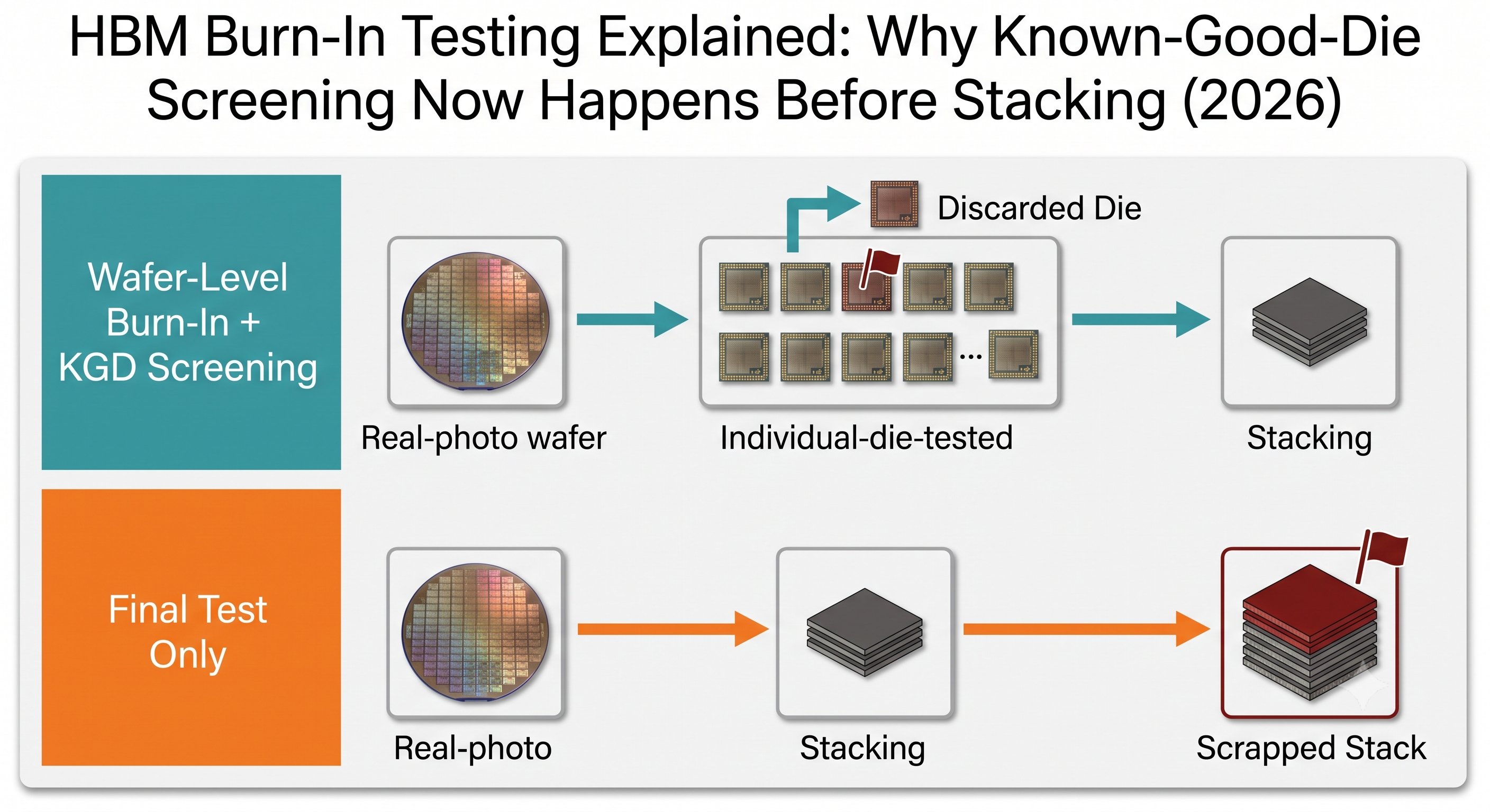
HBM burn-in and known-good-die (KGD) testing means every individual memory die is electrically stressed and screened at the wafer level — before it's thinned, singulated, or stacked — instead of waiting to find defects only after a finished HBM stack fails final test. The reason this matters is economic, not just technical: a single bad die inside an 8-to-16-high HBM stack can force the entire stack to be scrapped, and HBM now accounts for roughly half the total cost of an AI accelerator package. That's why HBM makers and test-equipment vendors have visibly shifted testing "left" — earlier in the manufacturing flow — rather than relying on final test alone to catch problems.
By The Whitepaper Skeptic — yield-economics work on an advanced-packaging project, plus HBM test-equipment tracking
Quick Facts
| Question | Answer |
|---|---|
| What does "known-good-die" (KGD) mean? | A die individually tested and verified to meet spec before it's committed to an expensive multi-die stack, rather than being tested only after stacking |
| Why test before stacking instead of after? | A single defective die can force scrapping an entire 8-to-16-high HBM stack; HBM now represents roughly half the total cost of an AI accelerator package |
| Who builds the wafer-level burn-in equipment? | Aehr Test Systems (FOX-XP systems — $14M order Feb 2026, $22M follow-on order Aug 2026, both from its "lead AI processor customer") and Teradyne (Magnum 7H tester, covering HBM2E through HBM4E) |
| How big is the KGD screening/test market? | Fact.MR, a paid market-research firm, estimates $1.6B in 2026 growing to $7.8B by 2036 (17.1% CAGR) — its own estimate, not an independently verified figure |
| Does this eliminate stack failures entirely? | No — wafer-level burn-in and KGD screening catch most defects before stacking, but some failure modes only emerge after dies are bonded together |
What "Known-Good-Die" Testing Actually Means
A "known-good die" is a die that has been individually tested — typically with both functional test and burn-in (electrical and thermal stress applied over time to surface latent defects that wouldn't show up in a quick functional pass) — and verified to meet spec before anyone commits further manufacturing cost to it. The concept isn't new to HBM specifically; it's long been standard practice in any packaging approach where a die gets permanently bonded to something else before it can be tested again.
What's changed with HBM is where that testing happens. HBM dies are stacked 8, 12, or 16 high, connected vertically through-silicon vias (TSVs) and microbumps whose pitch keeps shrinking with each generation (our CoWoS and hybrid bonding explainer covers this bonding step in more depth). Once a die is bonded into a stack, isolating and replacing just that one layer if it turns out to be defective is far more expensive — and often not practical at all — than catching the same defect before bonding. So the industry's practical answer has been to push burn-in and KGD screening earlier: to the wafer level, before dies are even thinned and singulated, rather than treating final test of the assembled stack as the primary screening gate.
Why HBM Testing Moved Left: The Stack Economics
The core argument for shifting test earlier is straightforward stack math: if you stack 12 dies and one of them is defective, you don't get "11 good dies and 1 bad one" — you typically get a scrapped stack, because the defect can compromise the whole assembly or make isolating the bad layer impractical after bonding. The more dies in a stack, and the more expensive each individual die and bonding step is, the more that math punishes finding defects late.
That cost pressure has grown alongside HBM's own economics. Industry coverage (SemiEngineering, FormFactor) frames it directly: HBM now accounts for roughly half the total cost of an AI accelerator package, so a scrapped stack isn't a minor yield hit — it's a meaningful hit to the economics of the whole package. Stack economics illustrate why the stakes keep rising further: TrendForce reporting (citing Korean industry sources The Elec and Dealsite) puts Samsung's redesigned 36GB, 12-high HBM4 pricing in the mid-$500 range — more than double the roughly $250 Samsung charged for HBM3E, per Notebookcheck's relay of that reporting — with SK hynix's HBM4 separately reported in a similar mid-$500 band in TrendForce's own November 2025 coverage of Samsung's price-parity push. Stack counts per package have climbed too: from 4 HBM2 stacks on the V100 (per Nvidia's own architecture specs, as documented by Cornell's GPU architecture teaching materials) to 8 HBM3E stacks on Blackwell (B200), confirmed by TechInsights' physical teardown analysis of the HGX B200 package, with Nvidia's Rubin generation reported at 8 HBM4 stacks totaling 288GB per package. More stacks per package simply means more opportunities for one bad die to sink an expensive assembly — consistent with the shift-left rationale industry coverage describes.
Yield-economics work on a Corning-related advanced-packaging project is where I learned to argue this in units of what gets thrown away rather than in percentage points, and it changes which numbers matter. At a mid-$500 12-high HBM4 stack against roughly $250 for HBM3E, the price of a scrap event roughly doubled in one generation while the screening step that prevents it did not — so a test that converts a stack's worth of scrap into a die's worth pays for itself at defect rates most yield charts would round down to noise. Put eight of those stacks on a single B200-class package and the number of chances to run that math per package goes up with it.
Industry trade coverage also describes SK hynix and other HBM makers as moving toward per-layer KGD enforcement rather than relying on final test of the completed stack alone — a framing consistent with the stack-economics argument above, though this specific claim is currently sourced to secondary trade coverage rather than a direct SK hynix or JEDEC statement.
Wafer-Level Burn-In vs. Final Test
| Aspect | Final test only (older approach) | Wafer-level burn-in + KGD screening (current shift-left approach) |
|---|---|---|
| When defects are caught | After the full stack is assembled and bonded | Before dies are thinned, singulated, or stacked |
| Cost of a caught defect | High — an entire multi-die stack may need to be scrapped | Lower — a single die is discarded before expensive packaging steps |
| What it screens for | Functional and structural defects present in the finished stack | Latent defects surfaced under electrical/thermal stress at the individual-die level, before bonding |
| Where it fits in the flow | End of the manufacturing line | Wafer level, ahead of thinning/singulation/stacking |
| Primary limitation | Doesn't catch a defect until after the most expensive steps are already sunk | Doesn't catch failure modes that only emerge after bonding (e.g., bonding-induced or stack-level thermal/mechanical stress) |
Neither approach fully replaces the other — most HBM makers still run some form of final test on the assembled stack. The shift is about which layer of screening carries the primary burden of catching defects, and moving as much of that burden as possible to the cheaper, earlier stage.
What Wafer-Level Burn-In Actually Catches (and What It Doesn't)
Wafer-level burn-in applies electrical and thermal stress to dies while they're still on the wafer, surfacing latent defects — weak transistors, marginal interconnects, and similar issues — that a quick functional test at room temperature and voltage might miss but that would likely fail in the field under real operating stress. This is the same underlying logic as burn-in testing in other high-reliability semiconductor segments, applied to HBM at the wafer level so it happens before the die is committed to a stack.
Precise, industry-wide figures for exactly what share of defects wafer-level burn-in catches before stacking are hard to pin down. The only specific breakdown found during research for this piece — a claimed ~85% pre-stacking defect capture rate, with remaining yield loss split roughly 18% die-level physical defects and 10% thermally-induced failures — traces to a single AI-generated aggregator report (Patsnap Eureka), not a named primary source such as a fab, JEDEC, or a named analyst or test-equipment firm, and no independent source could be found to corroborate those specific percentages. What industry coverage (SemiEngineering, FormFactor) does support qualitatively: KGD methodologies catch the large majority of die-level defects before stacking, and the yield loss that remains splits between defects intrinsic to the die itself (introduced during fabrication, thinning, or handling) and failures that only surface once thermal and mechanical stress is applied — some of which emerge only after bonding. Treat any specific percentage breakdown you encounter elsewhere as a single-source estimate, not an industry-consensus benchmark, unless it's attributed to a named fab, test-equipment vendor, or analyst firm.
What wafer-level burn-in structurally can't catch: failure modes that only emerge from the bonding and stacking process itself — thermal or mechanical stress introduced during stacking, or interconnect issues that only manifest once dies are physically joined. That's why some form of testing after stacking (sometimes described in the industry as known-good-stack-die, or KGSD, testing) still has a role even as more of the screening burden shifts earlier.
Who Makes the Equipment: Aehr FOX-XP and Teradyne Magnum 7H
Test-equipment demand is visibly following the shift-left trend. Aehr Test Systems has booked two large 2026 orders from its "lead AI processor customer" for fully automated FOX-XP wafer-level burn-in systems: a $14 million order in February 2026, followed by a $22 million follow-on order in August 2026, according to Aehr's own press releases. Teradyne markets its Magnum 7H tester specifically for HBM2E, HBM3, HBM3E, HBM4, and HBM4E base-die wafer test, memory-core test, and burn-in — including known-good-stack-die (KGSD) level testing, according to coverage of the product launch.
| Vendor / system | What it's built for |
|---|---|
| Aehr Test Systems — FOX-XP | Fully automated wafer-level burn-in systems; two 2026 orders ($14M Feb, $22M Aug follow-on) tied to an unnamed "lead AI processor customer" |
| Teradyne — Magnum 7H | Base-die wafer test, memory-core test, and burn-in across HBM2E through HBM4E, including known-good-stack-die (KGSD) level testing |
Both companies' product positioning tracks the same underlying trend described above: as HBM stacks get taller and per-die stakes get higher, demand for automated wafer-level and burn-in-capable test equipment has followed.
The KGD Test Market: Sizing Claims and How Much to Trust Them
Fact.MR, a paid market-research firm, publishes a "HBM Known-Good-Die (KGD) Screening & Test Market" report estimating the market at $1.6 billion in 2026, growing to $7.8 billion by 2036 — a 17.1% compound annual growth rate. This figure comes from a market-research firm's landing-page teaser for a paid report, not an independently verified industry figure, and it shouldn't be read as a settled number — it's Fact.MR's own estimate, offered here as one data point on how the market is being sized commercially rather than as confirmed fact.
It's worth treating any HBM KGD market-sizing number the same way: as one analyst firm's estimate rather than a consensus figure, unless corroborated by a second named source.
Where This Fits in the HBM Packaging Story
This piece sits alongside the other design, packaging, and interconnect explainers in our HBM/chiplet cluster, but covers a different angle: verification, not design. Our pillar article on HBM covers what HBM is and why it's stacked close to compute. Our HBM4 vs. HBM3E comparison covers what changes with HBM4's move to a logic-process base die and finer microbump pitch — both of which raise the stakes for per-die screening described here, since finer interconnects leave less margin for a marginal die to slip through undetected. Our CoWoS and hybrid bonding explainer covers the bonding/stacking step itself — the point after which a defective die becomes a much more expensive problem to isolate, which is exactly why testing has moved to happen before it. And our glass core substrate explainer covers a related materials-side response to the same size-and-density pressure driving HBM packaging decisions generally.
FAQ
Q: What is known-good-die (KGD) testing in HBM?
A: KGD testing means individually verifying each HBM die against spec — typically through functional test plus burn-in (electrical/thermal stress to surface latent defects) — before it's committed to a multi-die stack, rather than only testing the finished stack after it's assembled.
Q: Why does HBM testing need to happen before stacking, not after?
A: Because a single defective die inside an 8-to-16-high HBM stack can force the entire stack to be scrapped, and isolating a bad layer after bonding is far more difficult and expensive than catching the defect while the die is still on the wafer. With HBM now accounting for roughly half the cost of an AI accelerator package, catching defects late is a costly mistake.
Q: What's the difference between wafer-level burn-in and final test?
A: Wafer-level burn-in screens individual dies with electrical and thermal stress before they're thinned, singulated, or stacked. Final test happens after the stack is fully assembled and catches defects in the completed package — but by then, a defect typically means scrapping the whole stack rather than just one die. Most manufacturers now use both, with wafer-level burn-in carrying more of the screening burden than it used to.
Q: How big is the HBM known-good-die test equipment market?
A: Fact.MR, a paid market-research firm, estimates the HBM KGD screening and test market at $1.6 billion in 2026, growing to $7.8 billion by 2036 (a 17.1% compound annual growth rate). This is one firm's own market-sizing estimate rather than an independently verified figure.
Q: Does wafer-level burn-in catch every defect before stacking?
A: No. Wafer-level burn-in and KGD screening catch most known defect types before stacking, but some failure modes — particularly those introduced by the bonding and stacking process itself, such as stack-level thermal or mechanical stress — can only be detected after dies are physically joined, which is why some post-stacking testing (sometimes called known-good-stack-die, or KGSD, testing) still has a role.
Sources
- HBM Shifts Testing Left To Preserve AI Chip Yield — SemiEngineering
- High-Bandwidth Memory Testing — Why Early Test Strategies Are Critical for Yield, Cost, and Performance — FormFactor blog, 2026
- Aehr Receives $22 Million Follow-On Order for AI Processor Wafer-Level Burn-In Systems — Aehr Test Systems press release, Aug 2026
- Aehr Receives $14 Million Order from Lead AI Processor Customer for FOX-XP Wafer-Level Burn-In Systems — Aehr Test Systems press release, Feb 2026
- Teradyne Launches Magnum 7H Tester for HBM2E, HBM3, and HBM4 Devices — Embedded Computing Design
- HBM Known Good Die (KGD) Screening & Test Market Size — Fact.MR
- Nvidia May Raise Prices as It Pays Samsung Double for Future HBM4 AI Memory Modules — Notebookcheck (citing The Elec & Dealsite via TrendForce)
- Samsung Reportedly Targets HBM4 Price Parity with SK Hynix Amid Strong NVIDIA Demand — TrendForce, Nov 2025
- GPU Example: Tesla V100 — Memory and NVLink2 (four HBM2 stacks, 32GB) — Cornell Virtual Workshop, Cornell Center for Advanced Computing
- TechInsights' NVIDIA HGX B200 Analysis Reveals HBM3E Supplier and Advanced Packaging Innovation — TechInsights
- HBM4 and Fab Limits Prevent 1,000 Vera Rubin Racks Per Day in 2026 or 2027 — NextBigFuture
Author Bio
The Whitepaper Skeptic has direct project experience in semiconductor packaging strategy, including yield-economics and materials-vendor evaluation work on a Corning-related advanced-packaging project, and has continued tracking HBM test-equipment procurement trends (Aehr, Teradyne) as part of ongoing AI hardware packaging analysis.
Related Posts
- What Is HBM (High Bandwidth Memory)? A Beginner's Guide to AI Chip Packaging
- HBM4 vs. HBM3E: What Changed
- CoWoS and Hybrid Bonding Explained
- Glass Core Substrate Explained: Why Intel and TSMC Are Replacing Organic Chip Packaging (2026-2028 Timeline)
Tags
HBM burn-in testing, known-good-die testing, HBM test equipment, wafer-level burn-in, semiconductor test economics


Comments
Post a Comment