HBM4E Explained: What Changes When Custom Base Dies Arrive in 2027-2028
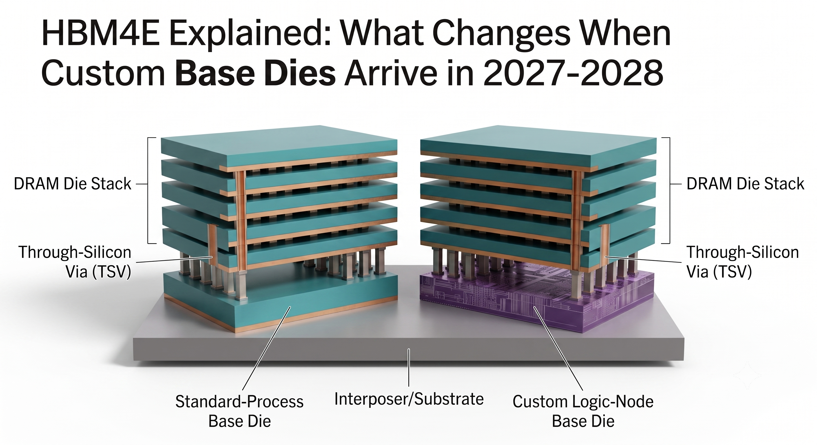
HBM4E is not a JEDEC-standardized memory generation — as of mid-2026, no unified JEDEC spec for HBM4E exists, unlike HBM4, which JEDEC finalized as JESD270-4 in April 2025. What actually defines HBM4E is a shift toward custom base dies: memory vendors are fabricating the logic base die under the DRAM stack on named third-party advanced-foundry logic nodes (TSMC's 3nm-class node via GUC, or Samsung's in-house 4nm) instead of a standard DRAM-line process. This article looks past HBM4's 2026 ramp to what changes in 2027-2028 — Micron's targeted mass-production entry, TSMC/GUC's roadmap speed target, and forecasts of how large a share of the HBM market HBM4E could take.
For the HBM4 vs HBM3E comparison that's already shipping today — the 1.05V voltage drop, JEDEC's decision to keep HBM4 on microbump packaging instead of hybrid bonding, and the base die's initial, unnamed shift toward a logic-class process — see our companion piece, HBM4 vs HBM3E: What Changed. This piece picks up exactly where that one left off: HBM4E is where base-die customization on named logic nodes stops being a directional trend and becomes an actual, differentiated product.
Quick Facts
| Question | Answer |
|---|---|
| Is there a JEDEC standard for HBM4E? | No unified JEDEC standard exists as of mid-2026 — a direct check of JEDEC's own press-release page shows only JESD270-4 (HBM4, finalized April 2025) and the in-progress SPHBM4 (a reduced-pin-count variant announced December 2025), with no finalized HBM4E standard listed |
| What's the core architectural change vs. HBM4? | The base logic die is fabricated on a named advanced foundry logic node (TSMC's 3nm-class node via GUC, or Samsung's in-house 4nm), not a standard DRAM-line process |
| When does mass production actually start? | Micron is targeting 2027 on its 1-gamma (1γ) EUV process; Samsung and SK hynix have already sampled 12-high HBM4E parts in 2026, ahead of full-volume production |
| How big could HBM4E be by 2027? | TrendForce has forecast HBM4E reaching roughly 40% of the 2027 HBM market — a figure TrendForce's own 2Q26 (May–June 2026) HBM market research continues to cite, about seven months after the original November 2025 estimate |
HBM4E vs. HBM4: Why There's Still No Single Standard
JEDEC generation cycles for HBM used to run on a multi-year cadence with a clear finalized spec at the center of each one — HBM3E, then HBM4 (JESD270-4, finalized April 2025), each with a single interoperable baseline every vendor built to. HBM4E breaks that pattern. According to TrendForce's reporting on the HBM roadmap, generation cycles have compressed to roughly 2.5 years, and vendors are increasingly moving ahead of JEDEC rather than waiting for it — HBM4E is the first generation where that gap is visible in shipping products rather than just conference-slide roadmaps. A direct check of JEDEC's own press-release archive as of mid-2026 confirms this: JEDEC's published releases cover JESD270-4 (finalized HBM4, April 2025) and the still-in-progress SPHBM4 (a reduced-pin-count, standard-package HBM4 variant announced in December 2025), but there is no press release announcing a finalized HBM4E standard.
Practically, that means "HBM4E" isn't one product — it's a label three different vendors are applying to three differentiated designs with different pin speeds, different process nodes for the base die, and different packaging choices. That's a meaningfully different situation than HBM4, where JEDEC's JESD270-4 spec gives every vendor's part a common electrical and mechanical baseline to compare against. If you're evaluating HBM4E parts from Samsung, SK hynix, and Micron side by side, you're comparing vendor roadmaps, not spec-sheet compliance to a shared standard.
The Real Change: Custom Base Dies on Named Logic Nodes
The headline story in most HBM4E coverage is pin speed and capacity. The more consequential story is where the base logic die gets built. On earlier HBM generations, the base die — the layer of logic that sits underneath the stacked DRAM dies and handles I/O, power management, and interfacing to the host processor — was fabricated on the same kind of process used for the DRAM dies above it. HBM4E changes that by moving the base die onto an advanced foundry logic node, decoupled from the DRAM process entirely.
TSMC and its ASIC partner GUC have detailed a "C-HBM4E" variant built around TSMC's N3P (3nm-class) custom base die. Per TrendForce's independent reporting on that announcement, the headline change is a voltage drop from 0.8V to 0.75V that TSMC says delivers roughly 2x the power efficiency of a standard-process DRAM base die. That builds on GUC's own primary tape-out announcement (April 2025) for the underlying HBM4 PHY and controller IP on the same N3P node — GUC's press release states that IP delivers 2.5x the bandwidth, 1.5x the power efficiency, and 2x the area efficiency of HBM3, with data rates up to 12 Gbps under all operating conditions. That's context on the die-level technology TSMC and GUC are now extending into custom HBM4E variants — it's a comparison against HBM3, not a C-HBM4E-specific 2027 benchmark, so treat any more specific "2027 pin-speed" figures attributed to this announcement with caution until TSMC or GUC publish one directly. Samsung is reportedly pursuing the same custom-base-die concept using its own in-house 4nm logic process rather than an external foundry, and SK hynix has reportedly been weighing TSMC's 3nm process for its own HBM4E logic dies as a way to compete with Samsung's in-house approach — as of a March 2026 TrendForce report, this was described as something SK hynix was considering, not a confirmed, finalized plan. Separately, Micron has partnered directly with TSMC to fabricate its HBM4E base dies rather than using an in-house DRAM-line process — a partnership Micron confirmed on its own fiscal Q4 2025 earnings call (September 2025) and reiterated as of TrendForce's May 2026 reporting: TSMC will manufacture both standard and custom HBM4E logic dies for Micron, with the custom option aimed at higher-margin, co-designed products.
Why does the fabrication location matter operationally, beyond bragging rights on a spec sheet? Having spent time on advanced-packaging materials work evaluating how design choices survive contact with a real qualification process, the base-die decision looks less like a marketing choice and more like a yield-and-co-design trade-off. Fabricating a DRAM vendor's base-die design on a third-party logic foundry's process node means qualifying that design against a process it wasn't originally built for — a real yield and schedule risk that has to be weighed against the payoff. That payoff is closer hardware-software co-optimization: a base die built on a modern logic node can carry more sophisticated power management, richer reliability logic, and potentially accelerator-specific logic that's co-designed with the GPU or ASIC it's paired with, instead of leaving all of that work to the host chip. That's the actual product HBM4E is selling — not just more gigabytes per second, but a memory stack whose logic layer can be engineered closer to the compute it serves. Our pieces on CoWoS and Hybrid Bonding Explained and UCIe Explained cover the interconnect and packaging side of that same co-design push in more depth.
Vendor Milestones: Don't Conflate Samsung's HBM4 and HBM4E Announcements
Coverage of Samsung's 2026 HBM announcements has a real risk of blurring two separate milestones together. They are not the same event:
| Vendor | Milestone | Date | What it actually is |
|---|---|---|---|
| Samsung | HBM4 mass-production shipment | 2026-02-12 | The already-standardized HBM4 generation (JESD270-4) entering volume production — this is HBM4, not HBM4E |
| Samsung | Industry-first HBM4E sample shipment | 2026-05-29 | A separate, later milestone: 12-high HBM4E samples at 16 Gbps/pin, 48GB, 3.6 TB/s per stack, reported at over 20% faster and over 30% higher capacity than HBM4 |
| SK hynix | 12-high HBM4E sample shipment | 2026-06-18 (reported) | 16 Gbps/pin samples, reported over 20% better power efficiency and 17% better thermal performance than HBM4, built on 1c/6th-generation 10nm-class DRAM with MR-MUF packaging |
| Micron | HBM4E mass-production target | 2027 | Targeting its 1-gamma (1γ) process — Micron's first EUV-lithography DRAM node; per TrendForce's May 2026 reporting on Micron's own remarks, the 2027 HBM4E ramp with TSMC (standard and custom logic dies) remains on track |
The roughly three-and-a-half-month gap (106 days) between Samsung's HBM4 mass-production date and its HBM4E sample-shipment date is itself informative: it shows Samsung treating HBM4E as a genuinely distinct product cycle layered on top of HBM4, not a minor spec bump. Samples are also not mass production — Samsung and SK hynix shipping 12-high HBM4E samples in mid-2026 means qualification and volume ramp are still ahead, not behind, them.
What Actually Changes in the 2027-2028 Window
Post 6 of this cluster covers what's shipping in 2026 — Rubin and MI400-class GPUs on HBM4. This piece is about what changes once that window closes:
- Micron enters mass production. Micron's HBM4E is targeted for 2027 on its first EUV-lithography DRAM node, putting Micron's HBM4E ramp roughly a year behind Samsung's and SK hynix's earlier sample shipments — a timeline TrendForce's May 2026 reporting on Micron's own statements confirms is still on track.
- Custom base-die efficiency and bandwidth gains keep climbing. TSMC/GUC's C-HBM4E roadmap centers on a custom N3P base die targeting roughly 2x the power efficiency of a standard-process design, building on GUC's underlying HBM4 PHY IP, which already delivers 2.5x the bandwidth of HBM3 on the same node — if the industry follows through on custom base dies at scale, this is the mechanism through which most of that additional performance actually gets delivered, not just wider interfaces.
- HBM4E could become the majority HBM product by then. TrendForce's forecast has HBM4E reaching roughly 40% of the 2027 HBM market — a figure its own 2Q26 (May–June 2026) market research continues to cite — which would make it the largest single generation in that year rather than a niche premium tier.
None of these are 2026 facts — they're the reason this generation is worth tracking now, before the products ship, rather than writing about it only after the fact.
FAQ
Q: What is HBM4E and how is it different from HBM4?
A: HBM4E is the generation that follows JEDEC-standardized HBM4, but unlike HBM4 it has no single finalized JEDEC standard as of mid-2026 — each vendor is building a differentiated design. The defining architectural change is a custom base logic die fabricated on a named advanced foundry logic node (TSMC's 3nm-class node via GUC, or Samsung's in-house 4nm) rather than a standard DRAM-line process.
Q: Is there a JEDEC standard for HBM4E?
A: No unified JEDEC standard for HBM4E exists as of mid-2026. HBM4 was finalized by JEDEC as JESD270-4 in April 2025, but HBM generation cycles have compressed to roughly 2.5 years and vendors are reportedly shipping HBM4E designs ahead of the standards body rather than waiting for a common spec.
Q: When will HBM4E enter mass production?
A: Timelines diverge by vendor. Samsung shipped industry-first 12-high HBM4E samples on 2026-05-29, and SK hynix followed with its own 12-high samples around 2026-06-18 — both are samples, not volume production yet. Micron is targeting 2027 for HBM4E mass production on its 1-gamma (1γ) EUV process.
Q: What is a custom base die in HBM4E?
A: It's the shift of the HBM base logic die — the layer that handles I/O and power management underneath the stacked DRAM dies — onto an advanced foundry logic process node instead of a standard DRAM-line process. This lets the base die carry more sophisticated logic and be co-designed more closely with the GPU or ASIC it pairs with, at the cost of qualifying a DRAM vendor's design against a foundry process it wasn't originally built for.
Q: How much of the HBM market will HBM4E take by 2027?
A: TrendForce has forecast HBM4E reaching roughly 40% of the 2027 HBM market, which would make it the largest single HBM generation that year. TrendForce's own 2Q26 (May–June 2026) HBM market research continues to cite this figure, about seven months after the original November 2025 estimate.
Sources
- JEDEC, "JEDEC® and Industry Leaders Collaborate to Release JESD270-4 HBM4 Standard: Advancing Bandwidth, Efficiency, and Capacity for AI and HPC" (official press release, April 2025)
- TrendForce, "HBM Evolution Outpaces JEDEC Standards as Generation Cycles Reportedly Shrink to 2.5 Years" (2025-09-01)
- TrendForce, "HBM4E Seen Hitting 40% of 2027 Market; Samsung, SK hynix Reportedly Aim for 1H26 Completion" (2025-11-13)
- TrendForce, "Micron Plans HBM4 Mass Production in 2026, Customized HBM4E to Launch in 2027-2028" (2024-12-23)
- TrendForce, "Samsung's Custom HBM4E Design Reportedly Aimed for Mid-2026, Parallels SK hynix and Micron" (2026-01-23)
- TrendForce, "SK hynix Reportedly Weighs TSMC 3nm for HBM4E Logic Dies to Gain Edge over Samsung" (2026-03-20)
- TrendForce, "Samsung Starts Shipping Industry-First HBM4E Samples Three Months After HBM4 Mass Production; Performance Up Over 20%" (2026-05-29)
- Samsung Newsroom, "Samsung Electronics Begins Shipment of Industry-First HBM4E Samples" (primary source)
- TrendForce, "SK hynix Ships 12-High HBM4E Samples, Boosts Bandwidth to 16Gbps and Power Efficiency by Over 20%" (2026-06-18)
- GUC (Global Unichip Corp.), "GUC Announces Tape-Out of the World's First HBM4 IP on TSMC N3P" (primary source, 2025-04-02)
- TrendForce, "TSMC Unveils Custom C-HBM4E Details: N3P Logic Dies Reportedly Target 2x Efficiency Gain" (2025-12-01)
- TrendForce, "Micron Counters HBM4 Speed Doubts with 11+ Gbps, Custom HBM4E Due 2027 with Higher Margins" (2025-09-24)
- TrendForce, "Micron More Upbeat on Outlook, Reportedly Sets 2027 HBM4E Ramp with TSMC for Standard, Custom Logic Dies" (2026-05-22)
- Our own pillar article: What Is HBM (High Bandwidth Memory)? A Beginner's Guide to AI Chip Packaging
- Our own cluster-mate: HBM4 vs HBM3E: What Changed
Author Bio
The Whitepaper Skeptic has direct project experience in semiconductor packaging strategy, including advanced-packaging materials work on a Corning-related project, and has spent time evaluating the yield and qualification trade-offs involved when a DRAM vendor's design has to be manufactured on a third-party foundry's logic process rather than an in-house line — the exact operational question HBM4E's custom base-die model is now raising industry-wide.
Related Posts
- What Is HBM (High Bandwidth Memory)? A Beginner's Guide to AI Chip Packaging
- HBM4 vs HBM3E: What Changed — the already-shipping 2026 generation comparison this article builds forward from; read that one for JESD270-4, the 1.05V voltage drop, and the microbump-vs-hybrid-bonding decision.
- CoWoS and Hybrid Bonding Explained: TSMC's Advanced Packaging Behind AI Chips
- UCIe Explained: The Open Standard Making Mix-and-Match Chiplets Possible
- Glass Core Substrate Explained: Why Intel and TSMC Are Replacing Organic Chip Packaging
Tags
HBM4E, HBM roadmap, semiconductor packaging, custom base die, AI chips


Comments
Post a Comment