Glass Core Substrate Explained: Why Intel and TSMC Are Replacing Organic Chip Packaging (2026-2028 Timeline)
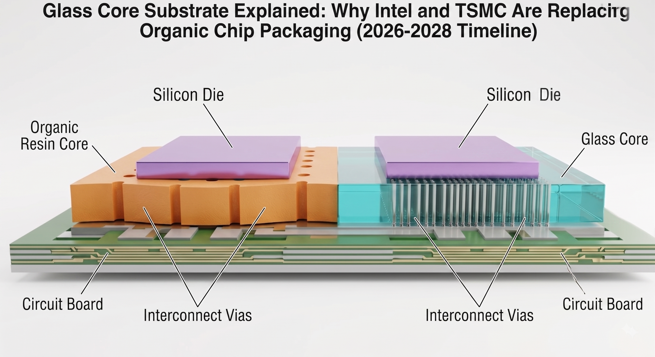
A glass core substrate replaces the organic resin (ABF/BT) core inside a chip package with a panel of glass, which stays flatter and expands less under heat than resin does — directly addressing the warpage and via-density limits that are now capping how large AI accelerator packages can get. Intel, TSMC, and Samsung Electro-Mechanics are all racing to move glass core substrates from pilot lines toward mass production, but the timing varies sharply by company: Samsung Electro-Mechanics is targeting 2H2027, while TSMC's own glass-core-substrate program — as distinct from its nearer-term CoPoS panel-packaging initiative, which uses a glass/organic hybrid structure and is on a faster 2H2028 track — isn't expected to reach commercial scale until after 2030, according to TrendForce. This article explains what a glass core substrate actually is, how it differs from both today's organic substrates and the separately-named "glass interposer," and lays out each company's real 2026 timeline — including where a widely-cited TSMC date actually belongs to a related but distinct program, rather than glass-core substrates themselves.
By The Whitepaper Skeptic — advanced packaging materials work on a Corning-related project, tracking glass-substrate roadmaps
Quick Facts
| Question | Answer |
|---|---|
| What is a glass core substrate? | A chip packaging substrate that swaps the organic (ABF/BT resin) core for a glass panel — lower CTE (thermal expansion mismatch), higher flatness, and sub-2-micron via density versus organic substrates |
| Why does it matter now? | AI accelerator packages have grown large enough that organic resin substrates are hitting warpage and interconnect-density limits — the same size-driven pressure covered in our CoWoS and HBM packaging spokes |
| Who's building it (2026 status)? | Intel (EMIB + glass-core sample shown at NEPCON Japan, Jan 2026, per industry press coverage; $3.3B India plant, 5-6 year buildout), TSMC (CoPoS pilot line at its VisEra subsidiary — a related glass/organic-hybrid panel-packaging effort, not full glass-core substrate), Samsung Electro-Mechanics (Sejong pilot line + Sumitomo-affiliated JV) |
| When does mass production start? | Samsung Electro-Mechanics' JV with Dongwoo Fine-Chem (a Sumitomo Chemical Group unit) targets 2H2027 — the nearest firm date among the three. TSMC's CoPoS panel-packaging initiative (a glass/ABF hybrid, not full glass-core) is on track for 2H2028 volume production, but TSMC's own full glass-core-substrate program isn't expected at commercial scale until after 2030, per TrendForce. Intel hasn't published a specific glass-core mass-production date |
| Is this the same as a glass interposer? | No — a different component with a different job inside the package. Commonly confused because both use glass, covered below |
What Is a Glass Core Substrate, and Why Organic Substrates Are Running Out of Room
Every chip package needs a substrate — a rigid base layer that sits between the silicon die and the printed circuit board, carrying the fine wiring that connects the die's tiny pads to the board's much larger ones, and mechanically supporting the whole package. For decades, that substrate has been built around an organic resin core, typically ABF (Ajinomoto Build-up Film) or BT (bismaleimide triazine) resin, sandwiched with copper wiring layers.
Organic resin has worked well for a long time because it's cheap, mature, and easy to manufacture at scale — the entire advanced-packaging supply chain is built around it. The problem is size. As AI accelerator packages have grown to fit more compute chiplets, more HBM stacks, and larger interposers (the same packaging pressure behind the CoWoS and chiplet integration trends we've covered elsewhere on this site), organic substrates are increasingly hitting two physical limits: warpage and via density.
Warpage happens because organic resin has a higher coefficient of thermal expansion (CTE) than the silicon die sitting on top of it — the two materials expand and contract by different amounts as the package heats and cools during operation, and at large package sizes that mismatch bends the substrate enough to stress or crack the interconnects. Via density is a separate limit: organic substrates can only pack interconnect vias (the tiny vertical conductors that route signals through the substrate) so tightly before manufacturing yield collapses, which caps how much wiring density a package can have.
Glass solves both problems structurally. It has a much lower CTE than organic resin — closer to silicon's own expansion rate — so it warps less at large package sizes. It's also inherently flatter and can support far finer via density (sub-2-micron, according to industry technical sources), which is what makes it attractive for the next generation of large, chiplet-dense AI packages rather than a smaller performance tweak on the current generation.
Glass Core Substrate vs. Organic (ABF/BT Resin) Substrate
| Property | Organic (ABF/BT resin) substrate | Glass core substrate |
|---|---|---|
| CTE (thermal expansion) match to silicon | Larger mismatch — a key driver of warpage at large package sizes | Much closer match to silicon — less warpage-driven stress |
| Flatness at large panel sizes | Degrades as package size grows — a known limiter for today's largest AI accelerator packages | Stays flatter at larger sizes — the core mechanical reason vendors are pursuing it |
| Via density / interconnect fineness | Practical limits around what today's advanced packages already use | Sub-2-micron via density achievable, enabling finer, denser interconnect |
| Manufacturing maturity (as of 2026) | Mature, high-volume, industry-standard supply chain today | Pilot lines only across all major vendors; no confirmed mass production yet |
| Cost at scale | Established, lower cost due to decades of process maturity | Currently higher — new equipment, new handling processes, not yet at scale economics |
Glass Core Substrate vs. Glass Interposer: Don't Confuse These Two
Both terms use "glass," which is exactly why they get mixed up — but they're different components doing different jobs. A glass core substrate replaces the entire organic core of the package substrate itself, the base layer the whole package sits on. A glass interposer is a separate, thinner intermediate layer that sits between the dies and the substrate, used specifically to route very fine, high-density connections between adjacent chiplets or between a die and HBM stacks — a role more comparable to the silicon interposers already used in some CoWoS-style packaging (covered in more depth in our CoWoS and hybrid bonding explainer).
In short: a glass core substrate is about replacing what the whole package sits on; a glass interposer is about a thin routing layer used for fine die-to-die or die-to-memory connections inside the package. A future package could, in principle, use both — a glass core substrate as its base and a separate interposer (glass or silicon) for die-level routing — but they are not the same component and are developed on largely separate roadmaps.
Who's Building What: Intel, TSMC, and Samsung's 2026 Timelines
All three major players are still at the pilot stage in 2026, not mass production — but their announced timelines, and how firmly those timelines are sourced, differ noticeably.
Intel has been the most public about its glass substrate push. At NEPCON Japan in January 2026, Intel reportedly demonstrated a "thick-core" EMIB-plus-glass-core-substrate sample described as having no micro-cracks (referred to in coverage as "No SeWaRe"). This claim comes from industry press that covered the event on-site — outlets including Wccftech, TechPowerUp, igor'sLAB, and EE News Europe, several of which cite each other's original reporting — rather than an Intel newsroom post or official NEPCON Japan session materials; no primary Intel statement specific to this NEPCON demo could be located as of this writing, so it should be read as well-corroborated trade-press coverage rather than a company-confirmed claim. Separately, and on firmer sourcing, Intel (with partner 3DGS) is building a $3.3 billion glass substrate plant in Odisha, India, with a reported 5-6 year buildout timeline, according to TrendForce's coverage of the project.
TSMC is running a pilot line for CoPoS (Chip-on-Panel-on-Substrate) at its VisEra subsidiary in 2026, targeting trial production in 2027 and volume production in 2H2028, per TrendForce. It's worth being precise about what that date covers: CoPoS is TSMC's nearer-term panel-level packaging initiative, and its early glass-related structure is a glass/ABF hybrid (glass layers paired with organic ABF material), not a full glass core. TSMC's own full glass-core-substrate program is a separate, later effort on TSMC's roadmap, and TrendForce places its commercial-scale production "likely after 2030" — years behind CoPoS. So the 2H2028 and "after 2030" dates aren't two conflicting estimates for the same thing; they're TrendForce's dates for two related but distinct TSMC programs (CoPoS first, full glass-core substrate later).
Samsung Electro-Mechanics is piloting glass core substrates at its Sejong plant and has formed a roughly ₩480 billion joint venture (tentatively named "GlaSSEM," majority-owned by Samsung Electro-Mechanics) with Dongwoo Fine-Chem, a Sumitomo Chemical Group unit, targeting 2H2027 for mass production at a new Pyeongtaek facility — according to TrendForce's coverage of the JV announcement, currently the most specific, nearest-term glass-core mass-production date among the three companies covered here.
For scale, one market-research estimate — from Semiconductor Insight, a smaller industry research aggregator — puts the glass core substrate market at roughly $920 million in 2026, growing to $1.87 billion by 2034 (a 9.3% compound annual growth rate). That figure is not from SEMI or Global Net Corp, despite sometimes being cited alongside their name; SEMI and Global Net Corp's own report on the same market instead projects a 67.2% compound annual growth rate from 2028 to 2040 without stating a comparable dollar figure — a dramatically different growth-rate estimate that underscores this is a single analyst's estimate rather than an industry consensus figure. Read the dollar figures above as directional, not precise.
Coming at glass from the materials-supply side on a Corning-related packaging program taught me to read these dates as procurement decisions rather than roadmap slides. The distance between TSMC's 2H2028 CoPoS volume date and its "likely after 2030" full glass-core date is not a rounding difference — they belong to two different sourcing plans, and I have previously collapsed two such dates into one because they arrived in the same deck. What sets the real date is qualification and second-source availability, neither of which a pilot-line demo tells you anything about.
Where Glass Substrates Fit in the AI Packaging Story
If you've been following the packaging side of AI chip design on this site, glass core substrates are the next chapter rather than a standalone topic. Our pillar article on HBM covers how memory gets stacked closer to compute; our chiplet vs. monolithic explainer and CoWoS and hybrid bonding piece cover how those stacks and chiplets get physically integrated into one package; and our UCIe explainer covers how chiplets from different vendors are meant to talk to each other once they're in that package. All of that — the stacking, the integration, the interconnect — sits on top of a substrate. Glass core substrates are the materials-science answer to a problem those other pieces created: as packages got bigger to fit more chiplets and more HBM stacks, the organic substrate underneath them started running out of flatness and via density to support it.
The same size-and-density pressure also shows up on the thermal side. Larger, denser packages concentrate more power in less area, which is a big part of why data centers are moving to liquid cooling — a trend we cover in our AI data center liquid cooling piece. Warpage and heat are related failure modes: a substrate that can't stay flat under thermal cycling is a substrate that's more likely to fail as packages run hotter, which is one more reason glass's lower CTE matters beyond just interconnect density.
FAQ
Q: What is a glass core substrate?
A: A glass core substrate is a chip packaging substrate that uses a panel of glass instead of organic resin (ABF/BT) as its core material. It offers a lower coefficient of thermal expansion, better flatness, and finer via density than organic substrates, which helps large AI accelerator packages avoid warpage and interconnect-density limits.
Q: What's the difference between a glass core substrate and a glass interposer?
A: A glass core substrate replaces the entire base layer the chip package sits on. A glass interposer is a separate, thinner routing layer used for fine die-to-die or die-to-memory connections inside the package, similar in role to the silicon interposers used in some CoWoS-style packaging. They're different components on largely separate development roadmaps.
Q: When will glass core substrates be in mass production?
A: Timelines vary by company. Samsung Electro-Mechanics, with its joint venture with Dongwoo Fine-Chem (a Sumitomo Chemical Group unit), is targeting 2H2027 — the nearest firm date. TSMC's nearer-term CoPoS panel-packaging initiative (a glass/ABF hybrid, not full glass-core) is targeting 2H2028 volume production, but TrendForce places TSMC's full glass-core-substrate program at commercial scale only after 2030. Intel has not published a specific glass-core mass-production date but is building a $3.3B glass substrate plant in India on a 5-6 year buildout.
Q: Why are organic substrates hitting limits for AI chips?
A: As AI accelerator packages have grown larger to fit more chiplets and HBM stacks, organic (ABF/BT resin) substrates are increasingly hitting warpage (from a CTE mismatch with the silicon die above them) and via-density ceilings that limit how much interconnect wiring the substrate can carry. Glass addresses both by staying flatter and supporting much finer via density.
Q: Is a glass core substrate the same as CoWoS?
A: No. CoWoS (Chip-on-Wafer-on-Substrate) is a packaging integration technique — a way of physically stacking and connecting dies — while a glass core substrate is a materials choice for the base layer underneath that packaging. TSMC's near-term panel-level initiative, CoPoS, is also a separate, earlier program from its longer-term glass-core-substrate roadmap; the two are easy to conflate but are tracked on different timelines.
Sources
- TrendForce Insights — Glass Substrate Development
- TrendForce Press Center — TSMC CoPoS / Glass Core Substrate
- TrendForce News — Intel Advances Glass Substrate Push With 3DGS, US$3.3 Billion India Plant Set for Five-to-Six-Year Buildout
- TrendForce News — Samsung Electro-Mechanics Reportedly Signs Deal to Form Glass Core JV With Sumitomo Unit, Targeting 2H27 Production
- IEEE Electronics Packaging Society — Glass Substrates Technical Primer
- Semiconductor Insight — Glass Core Substrate (for Advanced Packaging) Market Report, 2026-2034
- SEMI / Global Net Corp — Glass Core Substrate Market and Development Trends Report (press release)
Author Bio
The Whitepaper Skeptic has direct project experience in semiconductor packaging strategy, including advanced packaging materials work on a Corning-related project, and has continued tracking the glass core substrate roadmaps of Intel, TSMC, and Samsung as part of ongoing AI hardware packaging analysis.
Related Posts
- What Is HBM (High Bandwidth Memory)? A Beginner's Guide to AI Chip Packaging
- Chiplet vs Monolithic Chip: Why 2.5D/3D-IC Packaging Is Reshaping AI Chips
- CoWoS and Hybrid Bonding Explained
- UCIe Explained: The Open Standard Making Mix-and-Match Chiplets Possible
- AI Data Center Liquid Cooling: Why HBM and GPU Power Density Broke Air Cooling
- Panel-Level Packaging Explained: How TSMC's CoPoS Will Replace Round Wafers With Square Panels by 2028-2029
Tags
glass core substrate, semiconductor packaging materials, advanced packaging, Intel glass substrate, chip substrate technology


Comments
Post a Comment