Panel-Level Packaging Explained: How TSMC's CoPoS Will Replace Round Wafers With Square Panels by 2028-2029
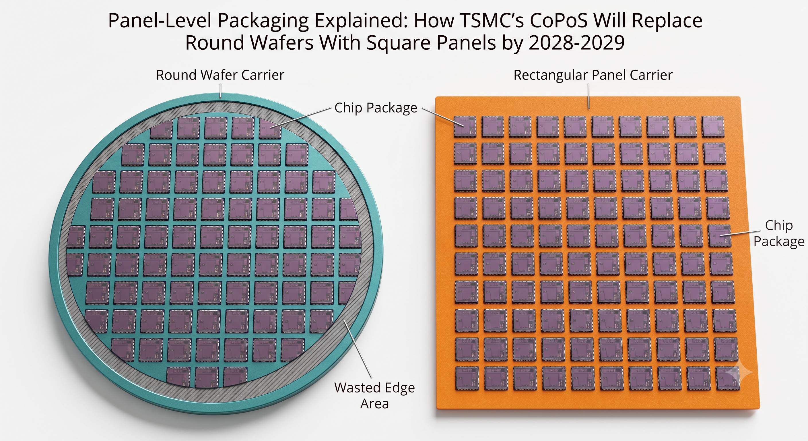
Panel-level packaging (PLP, also called FO-PLP) replaces the round 300mm silicon wafer used in today's chip packaging step with a large rectangular panel — eliminating the wasted edge and corner area of a circular format and enabling much bigger reticle sizes for AI accelerator packages. TSMC's version, called CoPoS (Chip-on-Panel-on-Substrate), uses a 310×310mm panel. TSMC launched an initial pilot line at subsidiary VisEra's Longtan facility, with a second pilot line following at TSMC's own AP7 fab in Chiayi; trade press reports through mid-2026 point to volume production landing somewhere in the 2028–2029 window (some outlets say late 2028, others say not before 2029) — with NVIDIA reported as the likely first customer. Samsung, ASE, and Powertech are already producing at panel scale today, several years ahead of TSMC's timeline.
By The Whitepaper Skeptic — semiconductor packaging strategy experience, Corning advanced packaging project
Quick Facts
| Question | Answer |
|---|---|
| What is panel-level packaging (PLP)? | The move from round 300mm wafer carriers to rectangular panels for the chip packaging step — more usable area per carrier, and larger achievable reticle sizes for AI packages |
| What panel size does TSMC's CoPoS use? | 310×310mm, per TrendForce and The Elec coverage of TSMC's roadmap — other vendors use different panel sizes (see below) |
| When is TSMC targeting CoPoS volume production? | Reports diverge — 2028–2029, after a 2026 pilot line at VisEra's Longtan facility and a second pilot at TSMC's AP7 (Chiayi); per DigiTimes, TrendForce, and Seoul Economic Daily |
| Who's already producing at panel scale? | Samsung (mobile AP/PMIC since acquiring the business from Samsung Electro-Mechanics in 2019, now extending to HPC/AI), ASE (300×300mm), Powertech (PiFO, since 2019) |
| How big is the PLP market? | Estimates vary sharply depending on scope — figures for "FO-PLP + glass substrate combined" and "PLP alone" are not directly comparable (see Market Size section) |
What Is Panel-Level Packaging, and Why Move Away From Round Wafers?
Today, the vast majority of advanced chip packaging happens on 300mm round silicon wafers — the same carrier format used earlier in the fab for the actual chip fabrication step. That format works fine for fabrication, where the wafer itself becomes the chips. But packaging is a different job: the wafer is just a temporary carrier that holds dies, interposers, and mold compound in place while they're processed and diced apart. A circle is a geometrically wasteful shape for that job, because you can only fit so many rectangular chip packages inside a circle before you're left with unusable curved edge and corner area.
Panel-level packaging swaps that round wafer carrier for a large rectangular (or square) panel. The same packaging processes — fan-out redistribution layers, mold compound, interconnect formation — run on the panel instead of the wafer. Two things change as a result: usable area per carrier goes up (less wasted edge), and the achievable reticle size — the maximum area a single chip package can occupy — goes up too, because panels can be made much larger than a 300mm wafer's usable rectangle.
That second point matters most for AI accelerators specifically. Modern AI chip packages already combine a large logic die with multiple HBM stacks side by side, and that combined footprint is bumping up against the reticle limits of wafer-based packaging. A bigger carrier with a bigger achievable reticle size means room for more HBM stacks and more logic in a single package — which is why PLP has become an AI-chip supply-chain story rather than just a packaging-format footnote.
TSMC's CoPoS: Panel Size, Timeline, and the NVIDIA Question
TSMC's panel-level packaging platform is called CoPoS — Chip-on-Panel-on-Substrate, extending the naming pattern of its existing CoWoS (Chip-on-Wafer-on-Substrate) platform, which our CoWoS and hybrid bonding explainer covers in more depth. According to independent trade press coverage — TrendForce, The Elec, DigiTimes, and Seoul Economic Daily all report consistent panel-size figures — CoPoS uses a 310×310mm panel. The rollout runs across two pilot phases rather than one: an initial pilot line at VisEra's Longtan facility, followed by a second pilot line at TSMC's own AP7 fab in Chiayi, which by August 2026 reporting had completed its production line and entered roughly a year of yield-stabilization work. From there, accounts diverge on the volume-production date: DigiTimes reported in mid-2026 that TSMC was targeting "not before 2029," while other coverage frames the window as 2028–2029 or, per the most recent DigiTimes reporting, potentially as early as 2028 if CoWoS capacity shortages and competitive pressure from Intel's rival packaging technology pull the timeline forward. No TSMC earnings-call transcript or Technology Symposium slide with these specifics turned up in research, so treat the panel size as well-corroborated across independent outlets and the production date as a moving target still being pinned down by trade press rather than TSMC itself.
NVIDIA has been widely reported as the likely first customer for CoPoS — but it's important to be precise about what that means. TrendForce's coverage frames this as an industry expectation based on NVIDIA's packaging demand and existing TSMC relationship, not a confirmed customer agreement. Treat "NVIDIA as first CoPoS customer" as reported anticipation, not an announced fact, until either company confirms it directly.
Panel-Level Packaging vs. Wafer-Level Packaging
| Aspect | Wafer-Level Packaging (today's standard) | Panel-Level Packaging (PLP/FO-PLP) |
|---|---|---|
| Carrier format | 300mm round silicon wafer | Large rectangular/square panel — size varies by vendor (e.g., 310×310mm for TSMC's CoPoS) |
| Usable carrier area | Reduced by wasted edge/corner area outside the largest rectangle that fits inside the circle | Higher — a rectangular carrier has little to no geometric waste |
| Achievable reticle size | Capped by wafer diameter — a known limit for today's largest AI accelerator packages | Larger — more room for combined logic + multi-HBM-stack packages |
| Manufacturing maturity (2026) | Mature, standardized equipment and process ecosystem across the industry | Newer at large scale; panel handling and warpage control still maturing, though several vendors are already in mass production |
| Who's producing at scale (2026) | Industry-wide standard | Samsung (mobile AP/PMIC, expanding to HPC/AI), ASE (300×300mm), Powertech (PiFO); TSMC's CoPoS is still pre-production |
The core trade-off: wafer-level packaging is the mature, universal default, while panel-level packaging trades some near-term process maturity for meaningfully larger usable area and reticle headroom — which is exactly the headroom AI accelerator packages are starting to need.
When I did advanced packaging materials work on a Corning-related project, the row that ended up mattering was not usable area but maturity. A 310×310mm rectangular carrier wins the geometry argument on paper by deleting the wafer's wasted corners, but every added millimeter of span makes flatness harder to hold through mold and redistribution-layer processing — which is why I now treat the "panel handling and warpage control still maturing" line in this table as the load-bearing one, not the area math.
Who Else Is Already in Panel-Level Packaging: Samsung, ASE, and Powertech
TSMC's CoPoS announcement has drawn most of the recent trade-press attention, but TSMC is not first to panel-scale packaging — it's catching up to competitors with a multi-year head start.
Samsung has quietly built up PLP capability for years. Samsung Electronics acquired the panel-level packaging business from Samsung Electro-Mechanics in April 2019, for roughly 785 billion won (about $580 million at the time) — a deal reported contemporaneously by Korean industry press. Samsung has applied the technology primarily to mobile application processors and power-management ICs since then, with more recent reporting indicating it's now extending the platform toward HPC/AI chip packaging.
ASE is already in mass production at panel scale, running a 300×300mm fan-out panel line in Kaohsiung — confirmed both by ASE's own technical publications and by independent trade coverage beyond TrendForce, and the company has said it's investing further to scale the format up toward 600×600mm. Powertech has its own platform, PiFO (Panel-level Integrated Fan-Out), in mass production since 2019 (corroborated by contemporaneous 2019 coverage in 3D InCites as well as more recent reporting from Semiconductor Engineering and TrendForce) and described in trade coverage as technically comparable to TSMC's CoPoS.
In short: by the time TSMC's CoPoS reaches volume production sometime in the 2028–2029 window, Samsung, ASE, and Powertech will already have several years of panel-scale production experience behind them — TSMC is bringing the largest foundry customer base to a format others got to first.
Format vs. Material: Why Panel-Level Packaging Is a Different Axis Than Glass Substrates
It's easy to mix up panel-level packaging with the separate shift toward glass substrates — trade coverage tends to blur the two, and TSMC's own CoPoS roadmap makes the overlap even easier to conflate, since CoPoS is explicitly headed toward glass-core panels over time.
But these are two independent axes of change. Panel-level packaging is about carrier format — round wafer versus rectangular panel — during the packaging step. Substrate material — organic resin versus glass — is a separate question about what the package's base layer is made of, covered in detail in our glass core substrate explainer. A chip can move to panel-level packaging now with an organic panel, and move to a glass panel later — the two transitions don't have to happen together, even though TSMC's own roadmap eventually combines them.
Keeping these separate matters for anyone tracking the packaging supply chain: a headline about a company adopting "panel-level packaging" is not automatically a headline about that company adopting glass substrates, and vice versa.
How Big Is the Panel-Level Packaging Market?
Market-size estimates for panel-level packaging vary sharply — and much of that variation comes down to scope, not disagreement about the underlying trend. One widely cited figure, from Counterpoint Research (DSCC), covers FO-PLP and glass substrate packaging combined, projecting growth from roughly $650 million in 2024 to over $8.1 billion by 2030. A narrower estimate from Yole Group, covering PLP alone, projects growth from about $160 million in 2024 to roughly $650 million by 2030 (a 27% CAGR). These are not the same market and shouldn't be merged into a single "the market will grow Nx" headline figure.
Separately, in an October 2025 report, Bloomberg Intelligence forecast that packaging costs for top-end AI chips "could climb to nearly $1,300 per chip in 2028" before falling roughly 45% by 2033 as panel-level packaging and mature 3D stacking approaches reset the cost curve — part of the same report projecting the overall advanced packaging market could reach roughly $80 billion by 2033.
Panel size itself is also inconsistently reported across sources — treat any single figure as vendor- or stage-specific rather than an industry standard. TSMC's CoPoS pilot runs at 310×310mm; ASE's current mass-production line runs at 300×300mm; 510×515mm is the size substrate makers most commonly cite as a mid-term industry favorite; and 600×600mm shows up both as ASE's own scale-up target and as the size of the glass panel Rapidus demonstrated for its separate glass-substrate packaging initiative (Amkor has discussed an even larger 650×650mm format). None of these should be read as a single agreed industry standard — each is tied to a specific company and production stage.
Where Panel-Level Packaging Fits in the AI Packaging Story
Panel-level packaging is the latest chapter in a packaging story we've been tracking across several spokes on this site. Our pillar article on HBM covers why stacking memory close to compute matters in the first place; our CoWoS and hybrid bonding explainer covers today's dominant wafer-based integration approach; and our glass core substrate explainer covers a parallel materials-side shift. Panel-level packaging sits alongside those as a third, largely independent lever — a change in carrier format rather than integration technique or substrate material — aimed at the same underlying problem: AI accelerator packages need more usable area and larger achievable reticle sizes than round 300mm wafers can comfortably provide.
It also connects directly to the capacity-allocation story in our advanced packaging market share comparison of TSMC, Samsung, and Intel: if PLP capacity scales as planned, it becomes another lever foundries can pull to expand advanced-packaging supply beyond what wafer-based CoWoS-class capacity alone can deliver.
FAQ
Q: What is panel-level packaging (PLP)?
A: Panel-level packaging is a chip packaging approach that uses a large rectangular panel instead of a round 300mm silicon wafer as the carrier during the packaging step. It reduces wasted edge/corner area and enables larger achievable reticle sizes, which matters for AI accelerator packages that combine large logic dies with multiple HBM stacks.
Q: What is TSMC's CoPoS?
A: CoPoS (Chip-on-Panel-on-Substrate) is TSMC's panel-level packaging platform, reportedly using a 310×310mm panel. TSMC ran an initial pilot line at subsidiary VisEra's Longtan facility, followed by a second pilot line at TSMC's own AP7 fab in Chiayi, with volume production reported for somewhere in the 2028–2029 window depending on the source, according to trade press coverage of TSMC's roadmap.
Q: How is panel-level packaging different from wafer-level packaging?
A: Wafer-level packaging uses a round 300mm silicon wafer as the carrier during packaging, which wastes some edge and corner area and caps the achievable reticle size. Panel-level packaging uses a rectangular panel instead, which reduces that waste and allows larger reticle sizes — more room for combined logic and multi-HBM-stack packages in a single unit.
Q: Is panel-level packaging the same as the shift to glass substrates?
A: No. Panel-level packaging is about carrier format (round wafer vs. rectangular panel) during the packaging step. The shift to glass substrates is a separate question about what material a package's base layer is made from (organic resin vs. glass). A chip can adopt panel-level packaging with an organic panel now and move to a glass panel later — the two transitions are independent, even though TSMC's own roadmap eventually combines them.
Q: Who is ahead in panel-level packaging — TSMC or its competitors?
A: By most current reporting, Samsung, ASE, and Powertech are ahead of TSMC in panel-level packaging. Samsung has applied PLP to mobile chips since acquiring the business in 2019 and is now extending it to HPC/AI; ASE and Powertech are both already in mass production at panel scale. TSMC's CoPoS platform isn't targeting volume production until sometime in the 2028–2029 window.
Sources
- The Elec — Intel and TSMC Push Panel-Level Packaging as Market Sets to Expand Tenfold
- DigiTimes — TSMC Fast-Tracks CoPoS: Whole Supply Chain Under Gag Order
- DigiTimes — Exclusive: TSMC Primes CoPoS Supplier Network for Chiayi, US Fabs Ahead of 2028 Ramp
- TrendForce — FOPLP Heats Up: ASE, Powertech Expand; TSMC Reportedly Preps 2026 CoPoS Pilot Line
- TrendForce — TSMC Advances Panel-Level Packaging, CoPoS Pilot Line Reportedly Set for June Completion, 2028–29 Ramp Eyed
- Seoul Economic Daily — TSMC Completes Line for Next-Gen CoPoS Packaging, Sees Year to Maturity
- Tech Times — TSMC Readies Panel-Level Packaging for AI Chips, Setting Up a Showdown With Samsung
- SammyFans — TSMC Prepares to Challenge Samsung's Lead in Panel-Level Packaging for AI Chips
- SemiEngineering — The Rise Of Panel-Level Packaging
- ETNews — Samsung Electronics Acquires PLP Business from Samsung Electro-Mechanics
- 3D InCites — Fan-Out Panel Production Becomes a Reality
- Yole Group — Is Panel-Level Packaging (PLP) Finally Emerging?
- Counterpoint Research — FOPLP and Glass Substrate Market Expected to Exceed $8 Billion by 2030, Driven by AI and HPC Demand
- Bloomberg Intelligence — Advanced Semiconductor Packaging Market Could Reach $80 Billion by 2033 as AI Chips Spread to Consumer Devices
- Persistence Market Research — Panel Level Packaging Market Size & Future Growth
Author Bio
The Whitepaper Skeptic has direct project experience in semiconductor packaging strategy, including advanced packaging materials work on a Corning-related project, and has continued tracking panel-level packaging's shift from round wafers to rectangular formats as part of ongoing AI hardware packaging analysis.
Related Posts
- What Is HBM (High Bandwidth Memory)? A Beginner's Guide to AI Chip Packaging
- CoWoS and Hybrid Bonding Explained: TSMC's Advanced Packaging Behind AI Chips
- Glass Core Substrate Explained: Why Intel and TSMC Are Replacing Organic Chip Packaging (2026-2028 Timeline)
- Advanced Packaging Market Share 2026: TSMC vs. Samsung vs. Intel's CoWoS-Class Capacity Compared


Comments
Post a Comment