Backside Power Delivery Explained: How Intel's PowerVia and TSMC's Super Power Rail Are Rewiring Chip Power in 2026
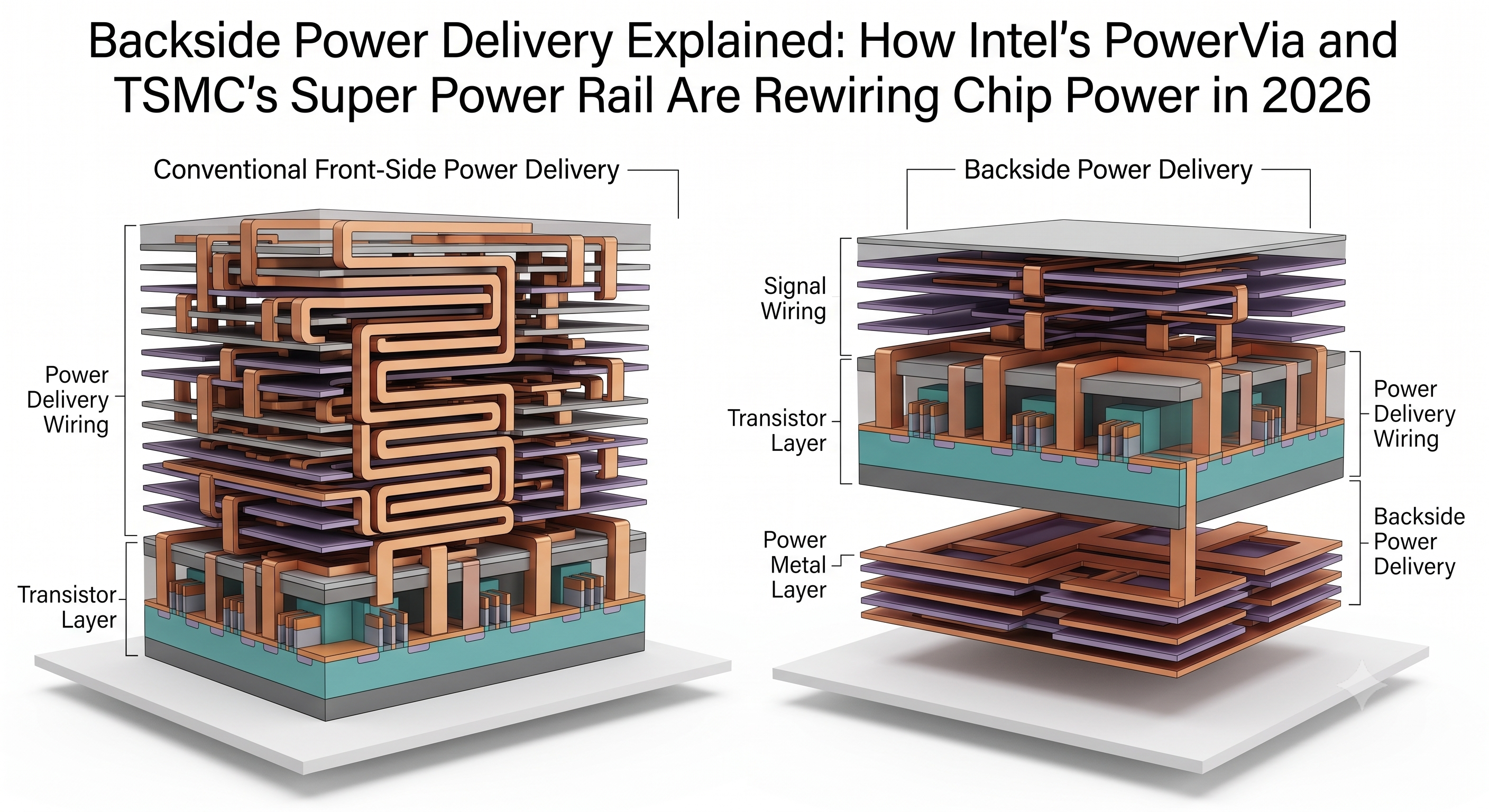
Backside power delivery moves a chip's power wiring to the reverse side of the wafer, separating it from the signal wiring that stays on the front — freeing up front-side routing space and cutting voltage drop as transistors keep shrinking. Intel shipped it first at volume, building PowerVia into the 18A node that powers its Panther Lake chip family starting in 2026. TSMC's competing implementation, Super Power Rail (SPR), is scheduled for the A16 node; TSMC says A16 begins mass production in Q4 2026, but at its April 2026 Technology Symposium the company clarified that actual volume-production ramp for customer products lands in 2027, timed to customer product schedules. Samsung's version won't arrive until its SF2Z node reaches mass production in 2027. This piece explains what backside power delivery actually changes, how the three implementations compare, and why it's a front-end wafer/transistor process — not a back-end packaging technique like CoWoS, hybrid bonding, or Foveros.
Quick Facts
| Question | Answer |
|---|---|
| What is backside power delivery? | Routing a chip's power rails on the back of the wafer instead of interleaving them with signal wiring on the front — frees up front-side routing space and reduces voltage (IR) drop |
| Who shipped it first, at volume? | Intel, with PowerVia built into the 18A node, powering Panther Lake chips starting in 2026 |
| When does TSMC's version arrive? | TSMC's Super Power Rail (SPR) is scheduled for the A16 node; TSMC targets Q4 2026 for mass-production start, but says (as of its April 2026 Technology Symposium) that full volume-production ramp for customer products follows in 2027 |
| When does Samsung's version arrive? | Samsung's SF2Z node, targeted for 2027 mass production — a separate node from its mobile-focused SF2/SF2P |
| Is it the same thing as CoWoS or hybrid bonding? | No — backside power delivery is a front-end wafer/transistor process. CoWoS, hybrid bonding, and Foveros are back-end packaging technologies applied after the wafer is fabricated |
What Backside Power Delivery Actually Changes
Every logic chip needs two kinds of wiring layered above its transistors: signal wiring, which carries data between transistors, and power wiring, which delivers voltage to them. For decades both have shared the same side of the wafer — the "front side" — stacked in interleaved metal layers above the transistors. As transistors have shrunk, that shared space has become a real constraint: power and signal wiring compete for the same limited routing area, and power delivery has to travel further and through more layers to reach transistors near the bottom of the stack, causing voltage (IR) drop that wastes energy and limits how tightly transistors can be packed.
Backside power delivery splits that shared space in two. After the front-side signal layers are built, the wafer is flipped, thinned, and a separate set of power-delivery layers is built into what was previously the back of the wafer — directly beneath the transistors instead of stacked above them alongside signal wiring. The result is a shorter, more direct path from the power supply to each transistor, freed-up front-side routing space that can now be used entirely for signal wiring, and (per vendor claims) higher performance and lower power at a given voltage. Intel's version of this technique is called PowerVia; TSMC's is called Super Power Rail; Samsung has not yet given its implementation an equivalent public brand name distinct from the SF2Z node itself.
Front-End Process vs. Back-End Packaging: Why BSPD Isn't CoWoS
The most common mix-up in coverage of backside power delivery is treating it as if it competes with, or overlaps, technologies like CoWoS, hybrid bonding, or Foveros. It doesn't — the two live at completely different layers of chipmaking, and a chip typically uses both without any conflict.
Backside power delivery is a front-end process: it changes how a single die's transistors are wired for power, and it happens at the wafer level, before the chip is diced and packaged. CoWoS (TSMC), hybrid bonding, and Foveros (Intel) are back-end packaging technologies: they determine how already-fabricated, already-diced dies — logic die, HBM stacks, chiplets — get physically connected and stacked together into a finished package, as covered in our CoWoS and hybrid bonding explainer. A chip fabricated on Intel's 18A node with PowerVia enabled can still go on to be assembled using Foveros 3D packaging — the two technologies are bundled into the same 18A products, but they operate on different sides of the fabrication process and don't substitute for each other. The same logic applies to TSMC: a chip built on the future A16 node with Super Power Rail can still be packaged with CoWoS or SoIC afterward. Backside power delivery decides how power reaches the transistors on one die; packaging decides how that die connects to everything around it.
This also answers a question worth asking directly: does backside power delivery work with CoWoS and HBM packaging? Yes — there's no structural incompatibility. A logic die using PowerVia or Super Power Rail is still a logic die from a packaging standpoint, and can be integrated with HBM stacks through CoWoS, hybrid bonding, or any other advanced-packaging approach exactly as a front-side-power die would be.
PowerVia vs. Super Power Rail vs. SF2Z: Side-by-Side Comparison
| Aspect | Intel PowerVia | TSMC Super Power Rail (SPR) | Samsung SF2Z |
|---|---|---|---|
| Process node | 18A | A16 | SF2Z (distinct from mobile-focused SF2/SF2P) |
| Status in 2026 | Shipping at volume in Panther Lake | Mass production targeted for Q4 2026; TSMC says (April 2026) full customer volume-production ramp lands in 2027 | Targeted for 2027 mass production |
| Claimed frequency/performance gain | ~6% frequency benefit, per Intel's own VLSI 2023 technical paper and Intel Newsroom release, measured on an internal PowerVia test chip prior to 20A/18A integration (not a claim about shipping Panther Lake silicon specifically) | 8-10% higher speed at the same power vs. N2P, per TSMC's own 2024 Technology Symposium materials and its VLSI 2026 technical presentation | 8% performance gain vs. SF2, per secondary reporting (TrendForce, Tom's Hardware, Guru3D) on Samsung's SFF 2024 roadmap presentation slides — Samsung's own published newsroom text confirms the PPA improvement directionally but does not itself publish the percentage figures |
| Claimed power reduction | Not separately broken out in available reporting | 15-20% lower power at the same speed vs. N2P, per TSMC's own Technology Symposium/VLSI 2026 materials | 15% power reduction vs. SF2, per the same secondary-reporting caveat as above |
| Other claimed gains | — | 8-10% chip-density gain, per TSMC's own materials | 7% area reduction vs. SF2, per the same secondary-reporting caveat as above |
| Manufacturing maturity | First to volume; yields were still ramping in early-to-mid 2026 but improved sharply through Q2-Q3 2026 — reported at roughly 65% good die yield in Q2 2026, climbing to roughly 85% by July 2026 (within about 5 points of TSMC N2's reported ~90%), a pace Intel's CEO has described as consistent with the industry-typical 7-8%/month improvement rate. These figures come from analyst/trade-press reporting (KeyBanc via TechTimes/BigGo Finance, TrendForce), not an official Intel disclosure, but they supersede earlier-2026 reporting that described yields as low as 20-25% and unlikely to reach "industry standard" before 2027 | Not yet in volume production as of this writing | Not yet in volume production as of this writing |
Intel's Head Start: PowerVia in Panther Lake, and the Yield Question
Intel is first to market with backside power delivery at volume, shipping PowerVia as part of the 18A node used in its Panther Lake chip family. Intel itself has cited a roughly 6% frequency benefit from PowerVia — stated in its 2023 VLSI Symposium technical paper and in an Intel Newsroom release ("PowerVia Test Shows Industry-Leading Performance"), based on an internal test chip built on a trial process ahead of PowerVia's later integration into 20A/18A, alongside a reported 30%+ improvement in platform voltage droop. That figure describes early internal test-chip results, not a claim about shipping Panther Lake silicon specifically.
Being first doesn't mean the transition has been smooth. Through late 2025 and early 2026, Intel's own executives described 18A yields as improving but still below the level needed for target margins, with CFO David Zinsner saying at the time that yields wouldn't reach "industry-acceptable" cost levels until around 2027. Since then, yields have moved quickly: analyst reporting (via TechTimes and BigGo Finance, citing a KeyBanc note, and corroborated by TrendForce) put good die yield at roughly 65% in Q2 2026, climbing to roughly 85% by July 2026 — closing to within about five percentage points of TSMC's N2 (reported around 90%) — a pace Intel CEO Lip-Bu Tan has described as consistent with the industry-typical 7-8%-per-month improvement rate. None of these more recent figures are official Intel disclosures, so they should be read as analyst estimates rather than confirmed company data, but they represent a materially better position than the "still ramping, still lagging" narrative that circulated in late 2025 and early 2026. Being first to ship a new process technology and having that process running at mature, high-volume yield are two different milestones — and by mid-2026, 18A's PowerVia rollout had largely closed the gap between them, even if it hasn't fully matched TSMC's yield yet.
Does Intel Actually Have a Process Lead Over TSMC?
One financial-commentary framing worth flagging by name: in a January 2026 Motley Fool piece (syndicated as-is to the Globe and Mail's markets section — the same single analysis, not two independent sources reaching the same number), contributor Timothy Green argued that, assuming TSMC's A16 entered volume production "as planned" by the end of 2026, Intel would hold "a head start of between 6-12 months" on backside power delivery. That figure is the author's own back-of-envelope framing built on the shipping-date gap between PowerVia (already in Panther Lake) and Super Power Rail (A16) — it is not an estimate published by Intel, TSMC, or an independent semiconductor-analysis firm, and it should be attributed as one analyst's opinion, not treated as settled fact. It's also worth noting the piece's own premise has since shifted: TSMC clarified at its April 2026 Technology Symposium that while A16 mass production still starts in Q4 2026, full customer volume-production ramp lands in 2027 — later than the "by the end of 2026" assumption the 6-12-month estimate was built on, which if anything stretches Intel's shipping-date head start rather than shrinking it.
It's worth being precise about what that framing is actually built on: Intel shipping backside power delivery in volume products before TSMC does. It says nothing on its own about which company has better yield, better cost-per-transistor, or a better long-term roadmap — questions where TSMC's manufacturing scale and historical execution track record still weigh heavily in the other direction, and where TSMC's Super Power Rail is aimed squarely at closing the exact gap Intel opened. Being first to ship a specific technique and having an overall process lead are not the same claim, and conflating them is the main way this story gets oversimplified in headline form.
What This Means If You're Choosing a Foundry or Evaluating Next-Gen Silicon
For chip designers and process-node buyers, the practical takeaway is less about who's "ahead" in the abstract and more about timing and risk tolerance. Intel's 18A with PowerVia is available now, and yield improved quickly through mid-2026 (from roughly 65% to roughly 85% good die yield between Q2 and July 2026, per analyst reporting) — a meaningfully better risk picture than it looked like in late 2025, though still trailing TSMC's mature N2 yield by a few points. TSMC's Super Power Rail on A16 begins mass production in Q4 2026 but, by TSMC's own April 2026 statement, doesn't reach full customer volume-production ramp until 2027 — arriving from a foundry with a long track record of hitting mature yield faster than rivals once a node ramps, which is exactly why some analysts expect TSMC to close the "who shipped it first" gap quickly once that ramp begins. Samsung's SF2Z, arriving a full node-generation later in 2027, is the one to watch if you're planning further out rather than choosing a node for 2026 production.
None of this changes packaging decisions downstream — as covered above, a chip's choice of backside power delivery implementation doesn't constrain which advanced-packaging path (CoWoS, hybrid bonding, Foveros, or otherwise) it can use afterward. The two decisions are genuinely separable, even though they're often bundled together in the same headline node announcements.
FAQ
Q: What is backside power delivery?
A: Backside power delivery is a chip manufacturing technique that routes a die's power wiring on the reverse side of the wafer instead of interleaving it with signal wiring on the front. This frees up front-side routing space for signal wiring and shortens the path power has to travel to reach each transistor, reducing voltage (IR) drop.
Q: Is backside power delivery the same as CoWoS or hybrid bonding?
A: No. Backside power delivery is a front-end wafer/transistor process that changes how a single die is wired internally. CoWoS, hybrid bonding, and Foveros are back-end packaging technologies that connect already-fabricated dies together after fabrication. A chip can use backside power delivery at the transistor level and still be packaged with CoWoS or Foveros afterward — the two aren't competing approaches.
Q: Does backside power delivery work with CoWoS and HBM packaging?
A: Yes. There's no structural conflict between the two. A logic die manufactured with backside power delivery (PowerVia, Super Power Rail, or Samsung's SF2Z implementation) is still a standard logic die from a packaging standpoint and can be integrated with HBM stacks through CoWoS, hybrid bonding, or other advanced-packaging methods just like a die using conventional front-side power delivery.
Q: When will TSMC's Super Power Rail be in volume production?
A: TSMC has targeted its Super Power Rail implementation for the A16 process node, with mass production starting Q4 2026 — but TSMC clarified at its April 2026 Technology Symposium that full customer volume-production ramp follows in 2027. Either way, this is after Intel's PowerVia, which is already shipping in 18A-based Panther Lake chips in 2026.
Q: Is Samsung's SF2Z the same as SF2 or SF2P?
A: No. SF2Z is a distinct process node from Samsung's mobile-focused SF2 and SF2P nodes, and it's the node where Samsung plans to introduce backside power delivery. SF2Z is targeted for 2027 mass production, roughly a year behind TSMC's A16/Super Power Rail timeline and after Intel's already-shipping PowerVia.
Sources
- PowerVia Test Shows Industry-Leading Performance — Intel Newsroom (primary source for the ~6% frequency figure)
- Backside Power Delivery Nears Production — SemiEngineering
- Intel Details PowerVia Backside Power Delivery Technology — Tom's Hardware
- TSMC unveils 1.6nm process technology with backside power delivery, rivals Intel's competing design — Tom's Hardware
- TSMC A16 Backside Power at VLSI 2026 — SemiWiki (TSMC's own 8-10% speed / 15-20% power / 8-10% density claims vs. N2P)
- TSMC Latest Roadmap: A12, A13 for 2029 Without High-NA EUV; A16 Volume Production Delayed to 2027 — TrendForce (April 2026 Technology Symposium)
- New Samsung 2nm roadmap shows backside power delivery coming in 2027 — TechSpot
- Samsung Unveils Next-gen 2nm Node Roadmap; SF2Z with Backside Power Delivery to Enter Production in 2027 — TrendForce
- Samsung Showcases AI-Era Vision and Latest Foundry Technologies at SFF 2024 — Samsung Semiconductor Global (primary source; confirms PPA improvement directionally, does not itself publish the 8%/15%/7% figures)
- Intel's 18A and 14A Bets Face Make-or-Break Year — Winbuzzer (CFO David Zinsner's late-2025/early-2026 "industry-acceptable by 2027" comments)
- Intel Foundry Hits 85% Yield, Winning Chip Orders as ASML Validates High NA EUV — Tech Times (July 2026, KeyBanc-sourced update superseding earlier low-yield reporting)
- Clash of the Foundries: Gate All Around + Backside Power at 2nm — SemiAnalysis
- The Chip Technology That Finally Gives Intel an Edge Over TSMC — The Motley Fool (single-author analyst opinion by Timothy Green, Jan 2026; also syndicated verbatim to the Globe and Mail's markets section — same analysis, not an independent second source)
Author Bio
The Whitepaper Skeptic has direct project experience in semiconductor packaging strategy, including advanced packaging materials work on a Corning-related project, and tracks process-node roadmaps like Intel's 18A and TSMC's A16 as part of ongoing AI hardware supply-chain analysis — with particular attention to where front-end transistor advances like backside power delivery intersect with the back-end packaging decisions covered elsewhere on this site.
Related Posts
- What Is HBM (High Bandwidth Memory)? A Beginner's Guide to AI Chip Packaging
- CoWoS and Hybrid Bonding Explained
- Who's Winning Advanced Packaging? TSMC, Samsung, and Intel's CoWoS-Class Capacity Compared
- Glass Core Substrate Explained: Why Intel and TSMC Are Replacing Organic Chip Packaging (2026-2028 Timeline)
- Custom HBM Base Die Explained: How TSMC, Samsung, and SK Hynix Are Redesigning HBM4E in 2026


Comments
Post a Comment