Inkjet-Printed OLED Explained: How TCL's $4.15B Bet Could Cut OLED Costs 35% While Samsung Says No
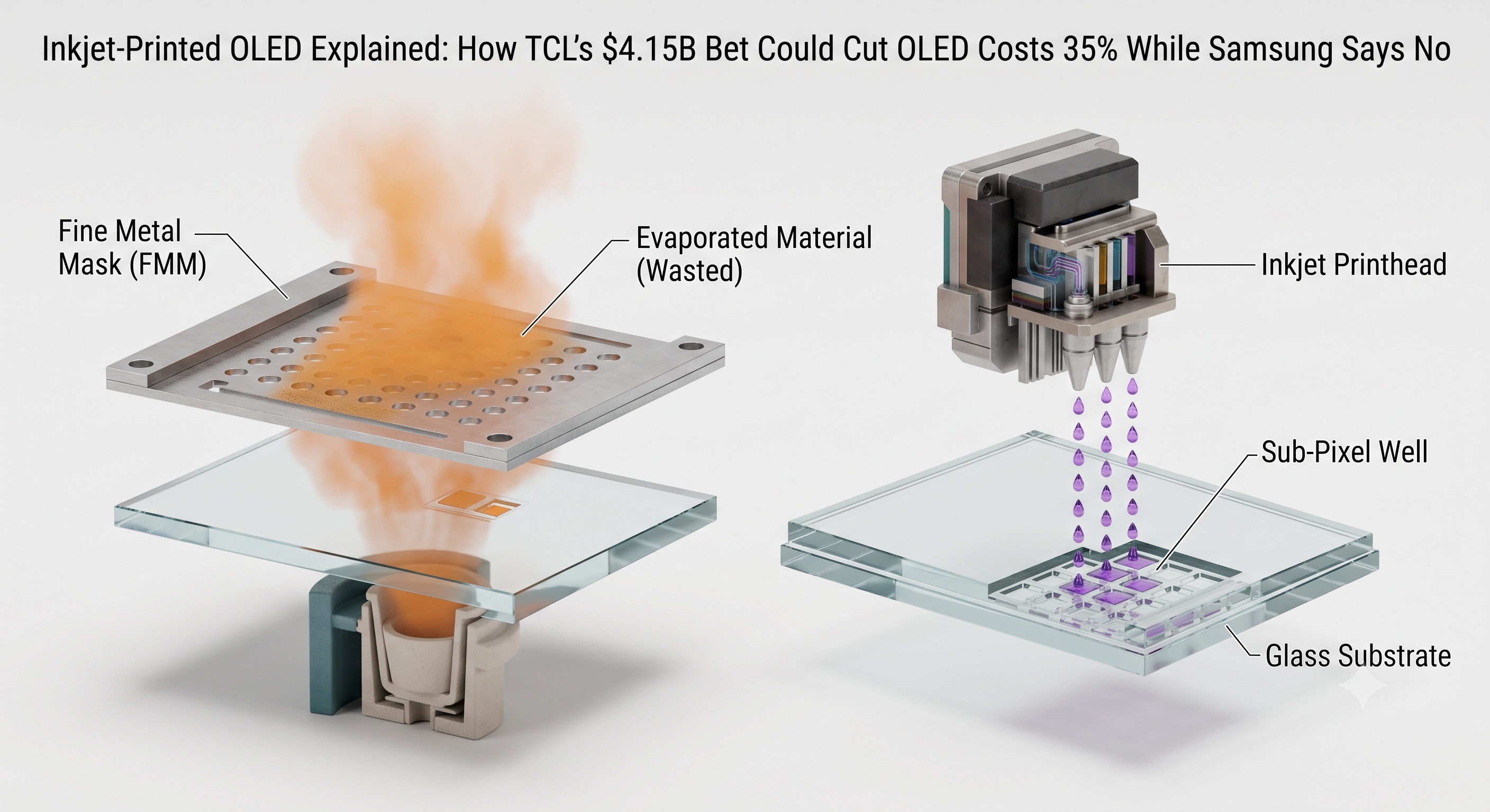
Inkjet-printed OLED (IJP OLED) manufacturing deposits organic emissive material directly onto glass through printhead nozzles, replacing the Fine Metal Mask (FMM) evaporation process that nearly every OLED panel shipping today still uses. TCL CSOT is the clear front-runner, already shipping small-scale product since late 2024 and now building a Gen 8.6 fab in Guangzhou to scale the process up. Samsung Display's own inkjet-printing record is more mixed than a simple "yes or no": it already relies on inkjet equipment for one layer of its QD-OLED panels, but in 2023 it tested and rejected a second inkjet vendor, Kateeva, for that same layer — and it still uses evaporation, not inkjet, for the RGB organic emissive layer that TCL's bet is actually built on. The two companies placing the biggest bets on OLED right now are taking genuinely different paths, but the difference is narrower and more specific than "TCL says yes, Samsung says no."
By The Whitepaper Skeptic — global materials supplier display-manufacturing project experience
Quick Facts
| Question | Answer |
|---|---|
| What is inkjet-printed OLED? | A deposition process that prints organic emissive material onto glass through nozzles, instead of evaporating it through a Fine Metal Mask (FMM) |
| Who's leading commercial production? | TCL CSOT — small-scale mass production from its Gen 5.5 Wuhan line since November 2024, plus a new Gen 8.6 fab under construction in Guangzhou |
| How much cheaper could it be? | Omdia estimates roughly 30-35% lower cost for inkjet-printed OLED notebook panels vs. FMM OLED — a separate, unrelated analyst estimate puts Gen-10 TV-scale inkjet panels 15-20% cheaper than WOLED |
| Is Samsung using inkjet printing? | Partially, and it's easy to misread — Samsung already uses inkjet printing (via Semes) for the QD color-conversion layer in QD-OLED, and in 2023 it also tested and rejected a second vendor, Kateeva, for that same QD layer. It doesn't use inkjet at all for the RGB organic emissive layer TCL is betting on — it uses evaporation there, same as almost everyone else |
| Has this been attempted before and failed? | Yes — Japan's JOLED spent over a decade on inkjet OLED R&D with TCL before filing for bankruptcy in March 2023, citing production delays and an inability to raise further funding |
What Is Inkjet-Printed OLED, and How Is It Different From FMM Evaporation?
Almost every OLED panel on the market today gets its red, green, and blue emissive material onto the glass substrate the same way: through thermal evaporation, with a Fine Metal Mask (FMM) — a precisely etched metal stencil — held just above the substrate to control exactly where each color lands. It's a mature, well-understood process, but it comes with two structural costs. First, a meaningful share of the evaporated material never reaches the substrate at all — it lands on the mask itself and is wasted. Second, as OLED substrates get physically larger (the entire reason the industry keeps moving to bigger "generation" sizes), a large metal mask starts to sag under its own weight, which makes hitting sub-pixel-level placement accuracy progressively harder to control at scale.
Inkjet printing removes the mask from the equation entirely. Printhead nozzles deposit precisely metered droplets of organic emissive ink directly into each sub-pixel well on the glass, the same basic principle as a desktop inkjet printer scaled up to industrial precision. Because there's no mask to waste material on, and no mask-sagging limit tied to substrate size, the pitch for inkjet printing has always been lower material cost and an easier path to larger substrates. The catch is that it introduces its own set of process-control problems that evaporation-based FMM doesn't have — more on that below.
TCL CSOT's Gen 5.5 Line and the New Gen 8.6 Guangzhou Fab
TCL CSOT began small-scale mass production of inkjet-printed OLED from its Gen 5.5 line in Wuhan in November 2024, the product of a decade-plus R&D partnership with Japan's JOLED. The company has since completed functional verification of its first real consumer product built on the process — a 27-inch 4K 120Hz stripe-RGB monitor panel rated at up to 300 nits brightness and 99% DCI-P3 color gamut, per OLED-Info's reporting — and is targeting mass production of that panel in July 2026.
To scale beyond that pilot-sized line, TCL broke ground on October 21, 2025 on a Gen 8.6 inkjet-printing fab in Guangzhou (internally referred to as T8) — a 29.5 billion yuan (roughly $4.15 billion) investment with a planned monthly capacity of 22,500 glass substrates, confirmed by TCL CSOT's own announcement as well as independent trade coverage from OLED-Info and Omdia's Display Dynamics research note. Notably, the fab is aimed at IT panels — laptops, tablets, and monitors — rather than TVs first, which puts TCL's initial commercial push in direct competition with the evaporation-based Gen 8.6 IT-panel lines Samsung Display and BOE are racing to bring online in the same window (our Gen 8.6 OLED fab race explainer covers that separate, evaporation-based capacity buildout in detail).
Why Inkjet Printing Could Cut Costs — Two Different Numbers, Not One
Cost claims around inkjet-printed OLED get repeated as a single figure in casual coverage, but the research actually points to two separate estimates with different scope, and conflating them overstates the case. Omdia's own research note (published May 2026) estimates that inkjet printing could cut costs roughly 30-35% for OLED notebook panels specifically, compared to conventional FMM OLED. A separate, analyst-sourced estimate, scoped to Gen-10 TV-size production, puts inkjet-printed 65-inch 4K panels only 15-20% cheaper than white-OLED (WOLED) — a smaller savings, on a different panel category, from a different source basis.
Separately, TCL itself claims roughly 2x material utilization compared to evaporation, on the logic that ink isn't wasted on a mask the way evaporated material is. That figure comes from TCL Central — it is TCL's own claim about its own process, and no independent third-party measurement of the specific "2x" figure was found in research, so it should be read as TCL's claim rather than an industry-confirmed number. None of these percentages should be read as a single settled "inkjet is X% cheaper" answer — they're three different claims, from three different sources, describing three different scopes of the same underlying technology.
In the materials and process evaluation work I did upstream of deposition-method decisions, a utilization figure was always the first thing I took apart. A roughly 2x material utilization advantage only turns into 2x lower material cost if the printable ink and the evaporable source material carry the same price per gram, and in the evaluations I sat in on they almost never did — which is how Omdia's 30-35% for notebook panels and the unrelated 15-20% figure for Gen-10 TV panels can both hold without either one confirming TCL's 2x number.
Why Samsung Rejected Kateeva — and Why It's Not About the RGB Emissive Layer TCL Is Betting On
The most counter-narrative part of this story is easy to overstate. Samsung Display reportedly tested inkjet printing equipment from vendor Kateeva and rejected it after the equipment received a "Fail" grade in Samsung's internal performance testing in late 2023, according to The Elec's original reporting. But the equipment Kateeva supplied was intended for the quantum-dot (QD) color-conversion layer in QD-OLED panels — the same layer Samsung already prints using equipment from Semes, a Samsung Electronics subsidiary — not the RGB organic emissive layer that TCL's Gen 8.6 bet is actually built on. Samsung's QD-OLED architecture doesn't use a patterned RGB organic emissive layer at all: it deposits a single, unpatterned blue emissive layer by evaporation and relies on the inkjet-printed QD layer above it to convert part of that blue light into red and green. So the Kateeva rejection is a real, sourced fact, but it's a rejection within a technology Samsung already uses in production (QD-layer inkjet printing) — not a rejection of inkjet printing for the RGB emissive layer TCL is betting its fab on.
It's worth stating the distinction plainly, because it's easy to collapse into a cleaner but inaccurate story. Samsung Display already uses inkjet printing in production today — via Semes, for the QD color-conversion layer — and it separately tested and rejected a second vendor, Kateeva, for that same QD-layer application, reportedly over performance shortfalls. None of that is evidence of how Samsung views inkjet printing for the RGB organic emissive layer, because Samsung has not publicly tested or deployed inkjet printing for that layer at all — its current QD-OLED architecture sidesteps the question entirely by using a single common blue emissive layer rather than patterned RGB emitters. The genuine difference between TCL and Samsung isn't "Samsung tested RGB emissive-layer inkjet printing and said no" — it's that Samsung's QD-OLED architecture doesn't need to answer that question, while TCL's Gen 8.6 bet is built directly on solving it. That's a narrower, more structural difference in approach than a head-to-head technology rejection, but it's still a real one, and it's part of why the two largest OLED players are currently making very different bets.
Samsung Display, meanwhile, continues to rely on evaporation-based FMM for the RGB organic emissive layer on its own next capacity expansion — a Gen 8.6 tandem OLED line reportedly tied to an Apple MacBook Pro contract, where trade press reported mass production commencing in July 2026 after earlier reports had pointed to a Q2 2026 start. That's simply the industry-standard evaporation process at work, not a decision Samsung has framed as a rejection of inkjet printing specifically. Our companion Gen 8.6 OLED fab race explainer covers that evaporation-based capacity buildout in more detail. Separately, our tandem OLED explainer covers the stacked-layer emissive structure Samsung and others are using on these evaporation-based lines — a structural choice that is independent of, and unrelated to, the inkjet-vs-evaporation deposition question covered here.
JOLED's Bankruptcy: A Cautionary Tale Underneath TCL's Bet
TCL's inkjet OLED program didn't start from scratch — it grew out of a decade-plus R&D partnership with JOLED, a Japanese company formed specifically to commercialize inkjet-printed OLED technology. JOLED filed for bankruptcy protection on March 27, 2023, with roughly $250-260 million in liabilities, according to Nikkei Asia's reporting — the company cited production delays, a costlier-than-expected path to stable output, and an inability to raise further funding as the immediate causes, after years of well-funded effort that never reached the commercial scale TCL is now attempting. That history matters for how skeptically to read TCL's current timeline: JOLED wasn't an underfunded startup trying and failing quickly — it was a serious, long-running industry attempt at exactly this technology, and it still didn't survive to commercial success on its own. TCL inheriting that R&D lineage is evidence of real technical progress, but it's also a reminder of how many well-resourced attempts at inkjet-printed OLED have already come up short before TCL's current push.
Inkjet Printing vs. FMM Evaporation at a Glance
| Factor | Inkjet Printing | FMM Evaporation |
|---|---|---|
| Deposition method | Printhead nozzles deposit metered ink droplets directly into sub-pixel wells | Organic material evaporated through a physical Fine Metal Mask stencil |
| Material waste | Little to no mask waste — TCL claims roughly 2x material utilization vs. evaporation (TCL's own claim, not independently verified) | Meaningful share of evaporated material lands on the mask itself and is wasted |
| Maturity | Early commercial stage — TCL CSOT small-scale production since November 2024 | Mature, standard process used for the large majority of OLED panels shipping today |
| Primary defect risks | Droplet placement accuracy, coffee-ring effect, non-uniform film thickness (mura) | Mask alignment/shadowing defects, mask degradation and sagging over repeated use and larger substrates |
| Substrate-size scaling | No mask-sagging limit — a cited advantage as substrates get larger | Mask sagging becomes harder to control as substrate generation size increases |
| Who's betting on it for the RGB emissive layer | TCL CSOT (aggressively, via its Gen 8.6 Guangzhou fab) | Samsung Display and LG Display continue to rely on it for the RGB OLED emissive layer |
What This Means for Defect Inspection
Inkjet printing doesn't just change how the emissive layer gets onto the glass — it changes what can go wrong with it, which is the direct bridge back to how fabs actually catch defects. Mask-based evaporation has its own well-understood failure modes, mostly tied to mask alignment and mask degradation over repeated use. Inkjet printing introduces a different set: droplet placement accuracy (did the ink land exactly in the intended sub-pixel well), the coffee-ring effect (ink that dries unevenly, depositing more material at the edge of a droplet than the center), and non-uniform film thickness that shows up downstream as mura — visible brightness or color unevenness across the panel.
None of that is a hypothetical concern once a fab is running inkjet at production volume rather than pilot scale — it's exactly the kind of sub-pixel-level defect our machine vision defect inspection explainer covers in more depth, and it's also directly relevant to how a fab's barrier and encapsulation choices interact with whatever defect profile the emissive layer itself produces, as covered in our OLED thin-film encapsulation explainer. A materials or process choice made at the deposition stage — inkjet vs. evaporation — determines which defect modes even exist further down the inspection line, the same "materials choice determines defect profile" logic that runs through this entire display-manufacturing cluster.
FAQ
Q: What is inkjet-printed OLED and how does it differ from FMM OLED?
A: Inkjet-printed OLED (IJP OLED) deposits organic emissive material directly onto glass through printhead nozzles, sub-pixel by sub-pixel. Conventional OLED manufacturing instead evaporates the material through a Fine Metal Mask (FMM), a physical stencil that controls where each color lands. Inkjet eliminates the mask and the material waste that goes with it, but introduces different defect risks, like droplet placement accuracy and uneven drying.
Q: Why did TCL invest billions in an inkjet OLED fab?
A: TCL CSOT is betting that removing the Fine Metal Mask cuts material waste and manufacturing cost significantly — Omdia estimates roughly 30-35% lower cost for inkjet-printed OLED notebook panels versus conventional FMM OLED — while also avoiding the mask-sagging problem that makes larger substrates harder to produce with evaporation. TCL began small-scale inkjet OLED production in 2024 and broke ground on a larger, roughly $4.15 billion Gen 8.6 fab in Guangzhou on October 21, 2025 to scale the process up to a planned 22,500 substrates per month.
Q: Why did Samsung reject Kateeva's inkjet printing technology?
A: Samsung Display reportedly tested Kateeva's inkjet printing equipment for the quantum-dot (QD) color-conversion layer in its QD-OLED panels — the same layer it already prints using equipment from Semes — and rejected Kateeva's equipment after it failed internal performance testing in late 2023, according to The Elec. That's a rejection within a technology Samsung already uses in production (QD-layer inkjet printing), not a rejection of inkjet printing for the RGB organic emissive layer that TCL's Gen 8.6 bet is built on. Samsung's QD-OLED architecture doesn't use a patterned RGB emissive layer at all, so the Kateeva episode doesn't tell us how Samsung views inkjet printing for that application.
Q: Is inkjet-printed OLED actually cheaper than traditional OLED?
A: The evidence points to lower cost in specific scopes rather than a single universal number. Omdia's estimate of roughly 30-35% lower cost applies specifically to notebook-panel production compared to FMM OLED; a separate, unrelated estimate for Gen-10 TV-scale production puts inkjet-printed panels only 15-20% cheaper than WOLED. TCL's own claim of roughly 2x material utilization versus evaporation is the company's own figure, not an independently verified measurement.
Q: When will inkjet-printed OLED panels be available in consumer products?
A: TCL CSOT has completed functional verification of a 27-inch 4K 120Hz stripe-RGB monitor panel and is targeting mass production in July 2026 from its existing Gen 5.5 Wuhan line, with its larger Gen 8.6 Guangzhou fab intended to scale IT-panel (laptop, tablet, monitor) production beyond that. Samsung Display, by contrast, is not pursuing inkjet printing for its own next-generation emissive-layer capacity, so any near-term consumer inkjet-printed OLED products are expected to come from TCL first.
Sources
- OLED ink jet printing: introduction and market status — OLED-Info
- TCL CSOT to start producing consumer 27" 4K inkjet-printed OLED panels in July 2026 — OLED-Info
- TCL breaks ground on massive new 8.6G OLED factory — FlatpanelsHD
- TCL CSOT Is Betting Big on Printed OLED With a Massive 8.6G Factory in the Works — TCL Central
- TCL CSOT Breaks New Ground in Display Tech with World's First 8.6-Gen IJP OLED Plant — TCL CSOT / PR Newswire
- Omdia: Inkjet printing to drive 30% cost reduction in OLED IT display manufacturing — Omdia
- Inkjet printing could cut OLED display costs by up to 35% — Engineering and Technology Magazine (IET)
- Reports suggest Kateeva's printers failed Samsung's QD printing tests, will not be used for QD-OLED production — OLED-Info
- Samsung Display rejects Kateeva's RGB inkjet equipment — The Elec
- Is Inkjet Printing the Answer to OLED Production Challenges? — Radiant Vision Systems
- Display maker JOLED files for bankruptcy with $250m in liabilities — Nikkei Asia
Author Bio
The Whitepaper Skeptic has direct project experience working with a global materials supplier on a display-related manufacturing project, including materials and process evaluation work that sits directly upstream of the deposition-method question covered here — the same lens applied to why TCL's cost claims and Samsung's rejection of inkjet printing should be read as two competing bets, not an industry consensus.
Related Posts
- How Are OLED and LCD Displays Manufactured? A Guide to Panel Fabrication and Inspection — pillar guide (mandatory pillar link for this spoke)
- Gen 8.6 OLED Explained: Why Samsung, BOE, and LG Are Racing to Build IT Panel Capacity in 2026 — the evaporation-based Gen 8.6 capacity race TCL's inkjet fab is directly competing against for the same IT-panel category
- Tandem OLED Explained: The Stacked-Layer Tech Set to Reach 36% of Laptop OLED Panels in 2026 — the stacked-emissive-layer structure Samsung and others are using on evaporation-based lines, a separate design choice from the inkjet-vs-evaporation deposition question covered here
- Machine Vision for Display Defect Inspection: How AOI and Deep Learning Catch Sub-Pixel Defects — how fabs actually catch the droplet-placement and mura defects unique to inkjet-printed panels
- OLED Thin-Film Encapsulation Explained: How Barrier Films Keep Flexible Displays From Dying in Days — a different materials-choice-determines-defect-profile lever in the same manufacturing cluster
Tags
inkjet-printed OLED, TCL CSOT, OLED manufacturing cost, Samsung QD-OLED, OLED deposition process


Comments
Post a Comment