OLEDoS Explained: How OLED-on-Silicon Microdisplays Are Powering the 2026 AR Smart Glasses Race
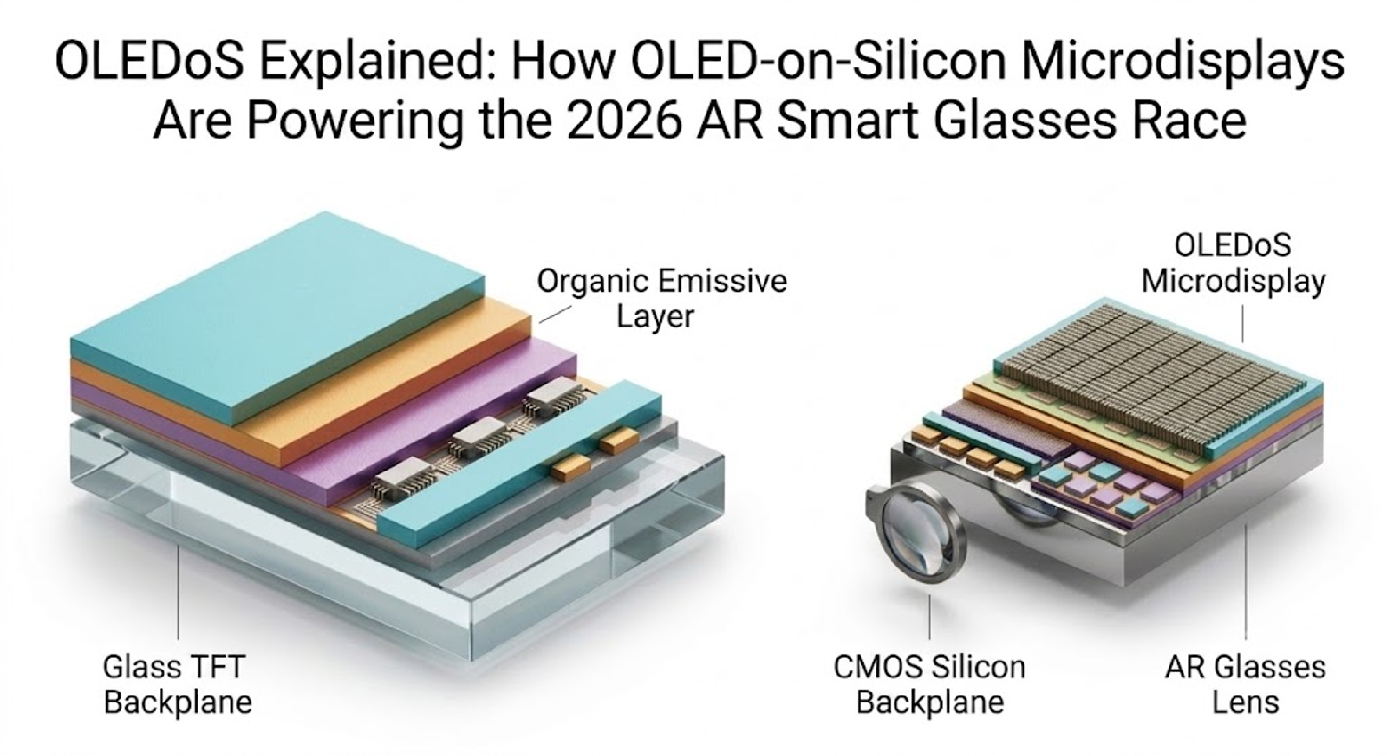
OLEDoS (OLED-on-silicon) is a microdisplay under 1 inch across, built by depositing OLED emitters directly onto a CMOS silicon wafer instead of a glass TFT backplane. That silicon backplane is what lets OLEDoS pack thousands of pixels per inch into a chip small enough to sit a few millimeters from your eye — which is exactly why it's become the display technology underpinning the 2026 AR smart-glasses wave. Samsung Display demonstrated a 1.3-inch RGB OLEDoS panel hitting 40,000 nits peak brightness at AWE USA in June 2026 — roughly double the 20,000-nit figure it showed at the same event a year earlier — and separately showed a 5,000 PPI, 1.4-inch RGB OLEDoS panel (15,000 nits peak brightness) at CES 2026 in January, both confirmed directly against Samsung Display's own newsroom releases. This piece explains how OLEDoS is actually manufactured, how it differs from microLED and from the large-panel OLED covered elsewhere on this blog, and why "this is a chip, not a panel" is the distinction that matters most for anyone evaluating the supply chain.
By The Whitepaper Skeptic — display materials work + semiconductor wafer-process analysis experience
Quick Facts
| Question | Answer |
|---|---|
| What is OLEDoS? | A microdisplay under 1 inch across, built by depositing OLED emitters directly onto a CMOS silicon wafer instead of a glass TFT backplane |
| How is it manufactured? | In a semiconductor fab on 200mm/300mm CMOS wafers using sub-micron photolithography — a front-end wafer process, not a glass flat-panel-display (FPD) process |
| What's the 2026 brightness/resolution ceiling? | 40,000 nits peak brightness (1.3-inch panel, AWE USA, June 2026) and a separate 5,000 PPI variant (1.4-inch panel, 15,000 nits, CES 2026, January) — both from Samsung Display |
| How big is the OLEDoS market? | Estimates vary meaningfully by report — $1.42B (DataVagyanik) to $1.76B (Mordor Intelligence) for 2026 |
| Who are the top vendors? | Samsung Display, LG Display, BOE, Sony Semiconductor Solutions, and eMagin are the vendors most consistently named as the leading competitive set |
What Is an OLEDoS Microdisplay, and Why "Silicon" Instead of "Glass" Matters
Every OLED display needs a backplane — the layer of driving circuitry underneath the emissive OLED material that switches each pixel on and off. In the large OLED panels covered in our display manufacturing pillar guide, that backplane is a thin-film-transistor (TFT) array built on glass. OLEDoS swaps that glass TFT array for a CMOS silicon wafer — the same kind of substrate used to fabricate logic chips and memory.
Silicon changes what's possible in two ways. First, CMOS fabrication supports far finer feature sizes than glass TFT processes, which is how OLEDoS panels reach pixel densities in the thousands-per-inch range instead of the hundreds-per-inch range typical of large-panel OLED — necessary when the display sits a few millimeters from the eye instead of an arm's length away. Second, it means an OLEDoS microdisplay is, structurally, a semiconductor die that happens to emit light rather than a shrunk-down version of a laptop or TV panel. Samsung Display's 2026 demos at AWE USA showed this scale directly: 0.62-inch and 1.3-inch panels, both smaller than a postage stamp, aimed squarely at AR smart glasses, defense optics, and AR head-up displays.
How OLEDoS Microdisplays Are Manufactured: A Chip Fab Process, Not a Panel Fab Process
This is the part of the OLEDoS story that most specs-and-marketing coverage skips, and it's the actual differentiator: OLEDoS is built in a semiconductor fab on 200mm or 300mm CMOS wafers using photolithography at sub-micron tolerances — closer in discipline to how a logic chip or a memory die gets made than to how a glass display panel gets made. That's the same "which fab discipline does this belong to" framing this blog has used to separate front-end wafer processes from back-end packaging steps in the backside power delivery explainer and the glass core substrate explainer — and it applies just as directly here, just one layer earlier in the process (wafer fab vs. panel fab, rather than front-end vs. back-end within a single wafer).
Inspection follows the same logic. Our machine-vision display-defect-inspection spoke covers automated optical inspection (AOI) at panel scale — catching sub-pixel defects across a glass substrate that can be a meter or more on a side. OLEDoS inspection happens at the opposite end of the scale: dead-pixel screening inside a semiconductor-grade cleanroom, at pixel pitches in the single-digit-micron range. Peer-reviewed literature confirms that OLEDoS fabrication requires cleanroom environments and advanced photolithography with tight alignment tolerances, but doesn't converge on one specific ISO cleanroom class across the industry — for reference, Fraunhofer IPMS's own OLED-microdisplay pilot line runs an ISO 14644-1 Class 5 cleanroom, not the stricter Class 1 sometimes cited in vendor marketing, and exact alignment-tolerance figures vary by fab rather than following one industry-wide spec. That's still the same cleanroom-class discipline semiconductor fabs apply to logic and memory dies, not the discipline applied to a glass FPD line.
Manufacturers describe OLEDoS yield as having improved substantially over the technology's history as fabrication processes have matured, though the industry does not publish a standardized, cross-vendor yield benchmark. A specific "roughly 70% a decade ago, climbing to 95%+ today" figure circulates in vendor marketing material, but it traces only to a single vendor blog and could not be independently corroborated against a stronger primary or trade-press source — treat the direction (yield has improved substantially) as reliable and the precise percentages as unconfirmed.
OLEDoS vs. MicroLED for AR Smart Glasses: What Actually Differs
OLEDoS and microLED microdisplays are the two technologies most often compared as candidates for AR smart-glasses waveguide projectors, and they get conflated often enough that the distinction is worth spelling out directly.
| Factor | OLEDoS (OLED-on-Silicon) | MicroLED Microdisplay |
|---|---|---|
| Backplane | CMOS silicon wafer | Typically silicon or a compound-semiconductor substrate (varies by maker) |
| Emissive material | Organic OLED material, deposited onto the wafer | Inorganic LED die, grown and then mass-transferred onto the backplane |
| Manufacturing maturity in 2026 | More mature — builds on an established CMOS + OLED deposition process flow | Less mature — mass-transfer yield remains the central bottleneck, as detailed in our MicroLED vs. OLED manufacturing-yield spoke (that piece covers large-panel MicroLED vs. OLED, but the underlying yield/process-maturity logic carries over to the microdisplay scale) |
| Brightness headroom | Up to 40,000 nits demonstrated at AWE USA, June 2026 (Samsung Display, 1.3-inch panel) | Higher theoretical brightness ceiling, but real-world output is currently constrained more by yield than by emitter physics |
| Where it's shipping in 2026 | AR smart glasses, camera viewfinders, some defense/AR-HUD programs | Mostly pre-commercial at microdisplay scale for AR; more traction in larger direct-view and automotive display formats |
The practical takeaway: OLEDoS is winning the near-term AR smart-glasses race less because it's the better emitter technology on paper and more because its manufacturing process is already closer to solved. MicroLED's brightness and lifetime advantages are real, but mass-transfer yield at microdisplay pixel densities remains the unresolved problem standing between microLED and commercial AR-glasses volume.
Samsung Display's 2026 Push: 40,000 Nits, 5,000 PPI, and the eMagin Acquisition
Samsung Display used AWE USA in June 2026 to show a 1.3-inch RGB OLEDoS panel reaching 40,000 nits peak brightness — roughly double the 20,000-nit figure it demonstrated at the same event a year earlier — plus a 0.62-inch RGB OLEDoS panel in prototype smart glasses; separately, at CES 2026 in January, it showed a 5,000 PPI, 1.4-inch RGB OLEDoS panel at 15,000 nits. Both sets of figures are confirmed directly against Samsung Display's own newsroom releases. Samsung is pairing that OLED-materials expertise with its acquisition of eMagin, a longtime U.S. microdisplay maker whose displays ship in aircraft helmets, head-up displays, thermal scopes, night-vision goggles, and AR/VR headsets — eMagin's own fourth-quarter and full-year 2022 results describe military programs, including the ENVG-B night-vision program and F-35 helmet-mounted-display shipments, as the primary driver of that year's 17% revenue growth, though the company has not published an exact military-revenue-share percentage — to push into defense, XR, and AR-HUD applications, a framing corroborated by multiple trade outlets covering the acquisition, including RoadtoVR, UploadVR, and DigiTimes.
Samsung Display, LG Display, BOE, Sony Semiconductor Solutions, and eMagin are the vendors most consistently named across current trade coverage as the top competitive set in OLEDoS — Mordor Intelligence's OLED Microdisplay Market report attributes roughly 65% of category revenue in 2024 to this top five.
How Big Is the OLEDoS Market? Why the Numbers Don't Agree
Market-research estimates for the 2026 OLEDoS/OLED-microdisplay market vary meaningfully by firm: $1.42B for 2026 growing to $6.59B by 2035 (18.6% CAGR) per DataVagyanik's OLED Microdisplay Market report, versus $1.76B for 2026 growing to $8.85B by 2031 (38.23% CAGR) per Mordor Intelligence's OLED Microdisplay Market report. That spread is worth taking at face value rather than averaging away — different research firms use different category definitions (some include AR-HUD and defense optics, others count only consumer AR/VR) and different forecast horizons (2031 vs. 2035), which is a more likely explanation than any one number being simply wrong.
A related, better-sourced pair of figures: IDC reported global smart-glasses shipments grew roughly 130% year-over-year in Q1 2026 — a figure that spans audio-only and AR/VR-capable eyewear together, with AR/VR-specific eyewear growing a more modest 85.9% YoY in the same period — while Omdia separately reported that AR/VR/MR near-eye display revenue, the category OLEDoS panels feed into, surpassed $1 billion for the first time in 2026, up more than 200% year-over-year. A frequently repeated "AR shipments +130% / OLEDoS market +200%" pairing circulates in secondary trade coverage, but traces back only to a single industry blog's citation of an unpublished analyst report and could not be independently confirmed — treat it as directionally consistent with the IDC/Omdia figures above rather than as an independently verified statistic in its own right.
SID (Society for Information Display) Display Week 2026 featured tandem-stack OLED and OLEDoS advances prominently in 2026 — for example, LG Display debuted its third-generation Tandem OLED at SID Display Week 2026, confirmed directly against LG Display's own press release — and secondary industry commentary has characterized 2026 as an inflection point for tandem structures reaching mass production. A specific claim that SID and SPIE jointly "designated" 2026 as the Tandem OLEDoS mass-production inflection point circulates in secondary trade coverage, but no such joint SID/SPIE publication could be located directly on either organization's own site; that framing should be treated as unconfirmed industry commentary rather than a citable SID/SPIE statement.
Tandem OLEDoS: Same Stacking Logic as Tandem OLED, Completely Different Substrate
Our Tandem OLED explainer covers tandem-stack OLED applied to laptop-sized glass panels viewed from arm's length — stacking two or more emissive layers, connected by a charge generation layer, to split the light-output workload and extend lifetime. Tandem OLEDoS applies the same underlying idea — multiple stacked emissive layers instead of one — to fingernail-sized silicon microdisplays viewed a few millimeters from the eye. The stacking logic is identical; almost everything else is not. The substrate is silicon instead of glass, the yield profile is governed by CMOS wafer economics instead of large-glass-panel economics, and the target market is AR/defense/XR hardware instead of laptops and tablets.
That's also why this piece treats OLEDoS as belonging to the same "front-end wafer process" family this blog has already mapped out on the semiconductor-packaging side — glass core substrate and backside power delivery both live at the wafer/transistor level of chipmaking rather than in back-end packaging or panel assembly. OLEDoS isn't a semiconductor-packaging technology in the same sense as those two, but it shares the same fab discipline and the same reason readers get it wrong: the marketing describes a display, but the manufacturing process describes a chip.
FAQ
Q: What is OLEDoS (OLED-on-silicon)?
A: OLEDoS is a microdisplay under 1 inch across, built by depositing OLED emitters directly onto a CMOS silicon wafer instead of a glass TFT backplane. The silicon backplane allows much higher pixel density than large-panel OLED, which is why OLEDoS is the leading display technology for AR smart glasses, camera viewfinders, and AR head-up displays in 2026.
Q: How is OLEDoS different from a regular OLED display?
A: Regular OLED panels (in phones, laptops, and TVs) use a glass thin-film-transistor (TFT) backplane and are made in a flat-panel-display (FPD) fab. OLEDoS uses a CMOS silicon wafer backplane and is made in a semiconductor fab using sub-micron photolithography — a fundamentally different manufacturing process, not just a smaller version of the same panel.
Q: OLEDoS vs. MicroLED — which is better for AR smart glasses?
A: OLEDoS currently leads in near-term commercial AR-glasses adoption because its manufacturing process builds on an established CMOS + OLED deposition flow. MicroLED has a higher theoretical brightness ceiling and better long-term lifetime characteristics, but mass-transfer yield at microdisplay pixel densities remains an unresolved bottleneck, which is why OLEDoS is shipping in more 2026 AR-glasses products today.
Q: How big is the OLEDoS market in 2026?
A: Estimates vary meaningfully by research firm — $1.42B for 2026 growing to $6.59B by 2035 per DataVagyanik, versus $1.76B for 2026 growing to $8.85B by 2031 per Mordor Intelligence — depending on how each report defines the category (consumer AR/VR only, vs. also including defense and AR-HUD applications) and which forecast horizon it uses.
Q: Who makes OLEDoS microdisplays?
A: Samsung Display, LG Display, BOE, Sony Semiconductor Solutions, and eMagin are the vendors most consistently named as the leading competitive set in current trade coverage. Samsung Display has been especially visible in 2026, showing 40,000-nit RGB OLEDoS panels at AWE USA and pairing its OLED-materials expertise with its eMagin acquisition to push into defense and XR applications.
Sources
- Samsung Display Unveils Ultra-Bright RGB OLEDoS for Smart Glasses at AWE USA — Tech Times
- Samsung Display Sets Sights on Next-Gen XR Innovations at AWE USA — Samsung Display Newsroom
- Samsung's latest XR display could make future smart glasses brighter and sharper — Android Authority
- Samsung steps up AR race with advanced microdisplay for smart glasses — KED Global
- OLED-on-silicon (OLEDoS) microdisplays: Technology challenges, design considerations, and adaptation in XR — ScienceDirect (peer-reviewed review)
- OLED Microdisplay Market Size, Trends, Share & Competitive Landscape 2031 — Mordor Intelligence
- Investigating the electrical crosstalk effect between pixels in high-resolution OLED microdisplays — PMC/NIH (peer-reviewed)
- OLED Microdisplay Market Size, Production, Price, Market Share — DataVagyanik
- Samsung Display Showcases OLED Innovations for the AI Era at CES 2026 — Samsung Display Newsroom
- OLED Microdisplay Cleanroom — Fraunhofer IPMS
- Samsung Acquires eMagin Microdisplay Maker, Citing "significant potential growth" of XR Devices — Road to VR
- Samsung Acquiring OLED Microdisplay Company eMagin For XR — UploadVR
- Samsung Display pushes forward with eMagin acquisition to open door to military XR market — DigiTimes
- eMagin Corporation Announces Fourth-Quarter and Full-Year 2022 Results — GlobeNewswire (eMagin investor disclosure)
- IDC: Global smart glasses shipments reached 3.566 million units in Q1 2026, up 130.1% year-over-year — IDC / futunn
- Near-eye display revenue will surpass $1bn for the first time in 2026, thanks to OLEDoS displays — Omdia
- LG Display Presents Future of Displays with Next-Generation OLED Technologies at SID Display Week 2026 — LG Display / PR Newswire
Author Bio
The Whitepaper Skeptic has direct project experience working with a global materials supplier on a display-related manufacturing project, and separately has spent time analyzing semiconductor packaging and front-end wafer processes — including CoWoS/hybrid bonding, backside power delivery, and glass-core substrate design — as part of ongoing AI hardware analysis. That combination is why this piece treats OLEDoS primarily as a CMOS wafer-fab product that happens to emit light, rather than as a shrunk-down version of a glass display panel — the distinction determines which yield, cleanroom, and inspection playbook actually applies.
Related Posts
- How Are OLED and LCD Displays Manufactured? A Guide to Panel Fabrication and Inspection — pillar guide
- Tandem OLED Explained: The Stacked-Layer Tech Set to Reach 36% of Laptop OLED Panels in 2026 — cluster-mate: same stacked-emissive-layer logic applied to large glass panels instead of silicon microdisplays
- MicroLED vs. OLED: Why Manufacturing Yield, Not Picture Quality, Decides the 2026 Winner — cluster-mate: the yield-vs-picture-quality framing this article applies to OLEDoS vs. microLED at microdisplay scale
- Machine Vision for Display Defect Inspection: How AOI and Deep Learning Catch Sub-Pixel Defects — cluster-mate: contrast point — panel-scale AOI inspection vs. the chip-scale, cleanroom AOI inspection covered in this article
- Glass Core Substrate Explained: Why Intel and TSMC Are Replacing Organic Chip Packaging — cross-cluster: shares the "front-end wafer process" framing this article reuses to distinguish OLEDoS's chip-fab discipline
- Backside Power Delivery Explained: How Intel's PowerVia and TSMC's Super Power Rail Are Rewiring Chip Power in 2026 — cross-cluster: same front-end wafer/transistor-level framing, applied to power delivery instead of microdisplay fabrication


Comments
Post a Comment