Custom HBM Base Die Explained: How TSMC, Samsung, and SK Hynix Are Redesigning HBM4E in 2026
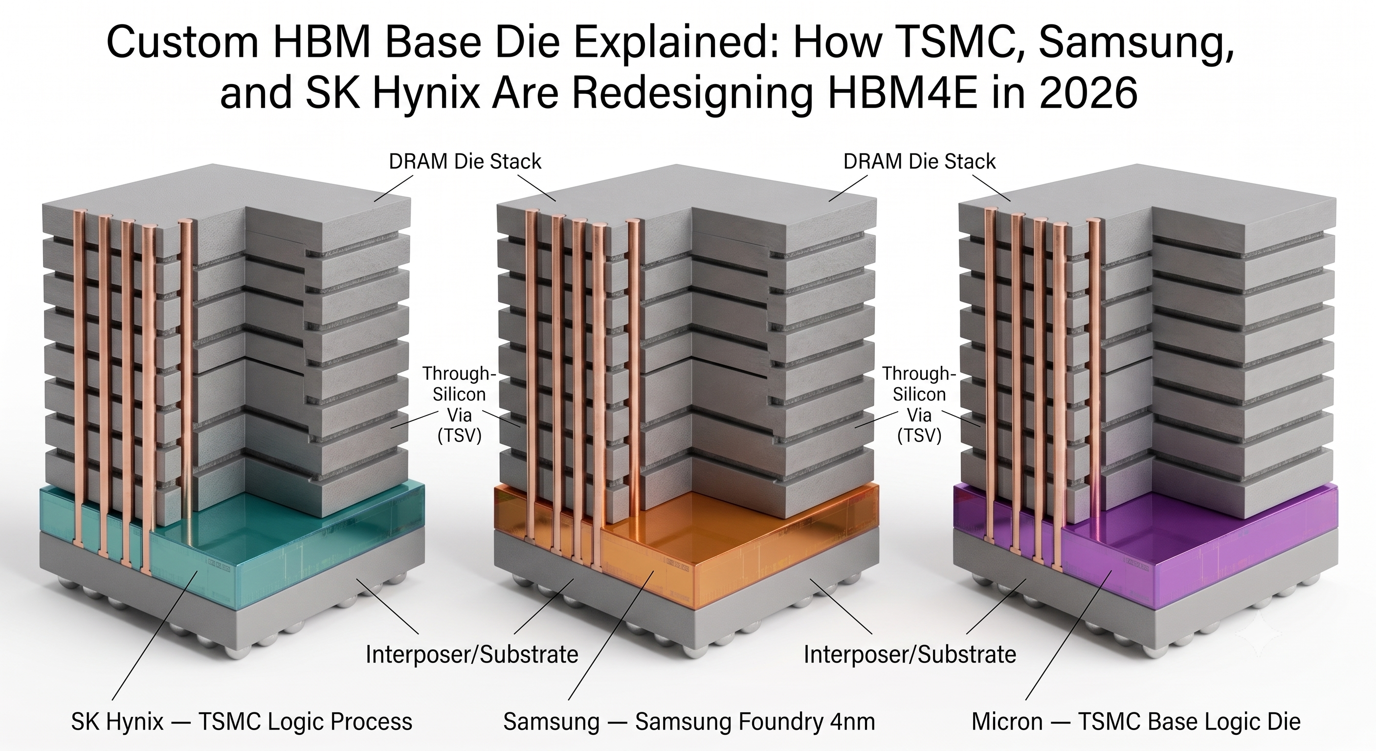
A custom HBM base die is the logic layer sitting beneath the DRAM stack in an HBM module — the part that handles I/O, power delivery, and system management — now being moved off the same commodity DRAM process the memory dies use and onto dedicated, customizable logic processes, starting with HBM4E. SK Hynix, Samsung, and Micron are each taking a different foundry-and-node path to get there, and the choices matter competitively because they determine how closely a memory maker can tailor its HBM stack to a specific hyperscaler's accelerator design. Samsung's own May 2026 announcement confirms its HBM4E base die runs on Samsung Foundry's 4nm logic process, distinct from the 2nm process Samsung has separately said it's reserving for the following generation, HBM5.
By The Whitepaper Skeptic — packaging strategy experience, tracking foundry-logic and DRAM convergence in HBM4E
Quick Facts
| Question | Answer |
|---|---|
| What is a base die? | The logic layer at the bottom of an HBM stack, underneath the DRAM dies — it handles I/O/PHY to the host processor, power management, and DRAM sequencing, connected to the DRAM layers above it via through-silicon vias (TSVs) |
| What's changing with HBM4E? | The base die is moving off the shared DRAM process it was historically built on and onto dedicated, foundry-made logic processes that can be customized per customer — a structural break from earlier HBM generations |
| SK Hynix's approach (reportedly) | TSMC ~12nm for mainstream server parts, TSMC 3nm for premium logic dies aimed at Nvidia GPU and Google TPU sockets — per TrendForce, March 2026, not confirmed directly by SK Hynix |
| Samsung's approach | Samsung Foundry's 4nm logic process for the HBM4E base die, confirmed directly by Samsung (Samsung Newsroom, May 2026); Samsung is separately targeting 2nm for the following generation, HBM5 |
| Micron's approach | Tapped TSMC to fabricate its HBM4E base logic die, but targeting 2027 production (later than SK Hynix/Samsung) and, per TrendForce, sticking with its existing DRAM process for the near term for cost reasons |
What Is a Base Die, and Why Wasn't It Customizable Before?
An HBM module is a stack of DRAM dies connected vertically by through-silicon vias, sitting on top of one more die at the bottom of the stack — the base die (also called the logic die or buffer die). The base die doesn't store data itself; its job is to manage everything around the DRAM: the I/O and physical-layer (PHY) interface that talks to the host GPU or accelerator, power delivery and thermal management across the stack, and command/address routing to the DRAM layers above it. If you've read our pillar explainer on HBM, this is the piece of the stack that sits between "how HBM is wired together" and "how it actually talks to the rest of the package."
For every HBM generation through HBM3E, the base die was manufactured on the same DRAM process node as the memory dies stacked on top of it. That wasn't because a DRAM process is well-suited to logic — DRAM processes are optimized for capacitor density and refresh behavior, not for the transistor switching speed and power efficiency that logic circuits want. It was a manufacturing simplification: keeping the whole stack on one process kept the supply chain and yield model simple, and the compromise on I/O logic performance wasn't yet the bottleneck holding accelerators back.
Why Hyperscalers Are Pushing to Customize the HBM4E Base Die
That compromise stops making sense once the base die becomes a customization lever rather than a fixed commodity part. Building the base die on a dedicated foundry logic process — separate from the DRAM stack above it — opens up two things memory makers couldn't previously offer: a logic process actually optimized for I/O switching speed and power efficiency, and a customization surface that a hyperscaler or accelerator vendor can co-design with the memory maker for their specific chip, interposer, and power budget rather than accepting a one-size-fits-all part.
Marvell — a vendor that sells custom-silicon and HBM PHY IP, and therefore has a direct commercial interest in this narrative — has published its own estimates for what a custom base die can deliver: up to a 33% increase in effective memory capacity, a 70% reduction in I/O power, and roughly 25% more silicon area freed up on the base die (previously occupied by generic, non-optimized I/O logic), which Marvell projects could make custom silicon roughly 25% of the accelerated-compute silicon market by 2028. These are Marvell's own marketing and analysis figures, not independent analyst numbers, and should be read with that commercial context rather than as neutral industry consensus.
In packaging strategy work I ended up sorting numbers like these by a single question: who has to be right for the figure to hold? Marvell's 33% effective-capacity gain and 70% I/O power reduction are per-design engineering claims, checkable against one accelerator's actual power budget by anyone with the design in front of them. The projection that custom silicon reaches roughly 25% of the accelerated-compute market by 2028 is a different species — a market forecast published by a company selling the base-die IP that forecast assumes everyone buys — and the two do not earn equal weight just because they arrive in the same sentence.
JEDEC's HBM4 standard (JESD270-4) is reported by trade press, including Tom's Hardware, to formalize support for a customizable base-die option as part of the finalized spec — a structural signal that base die customization is now a standards-sanctioned part of HBM4-generation design, not just an ad hoc practice layered on top of an otherwise-silent standard. If you need the exact clause language for a technical spec review, check JEDEC's own published standard rather than relying on secondary summaries.
HBM4E Base Die Process Node Comparison: SK Hynix vs. Samsung vs. Micron
| Memory maker | Foundry / process (reported) | Target segment | Production timing | Sourcing confidence |
|---|---|---|---|---|
| SK Hynix | TSMC ~12nm (mainstream), TSMC 3nm (premium) | 12nm for mainstream server parts; 3nm reportedly aimed at Nvidia GPU and Google TPU sockets | Not specified in available reporting | TrendForce, "reportedly" — not confirmed by SK Hynix directly |
| Samsung | Samsung Foundry 4nm (confirmed) | Custom HBM4E base die design | Design completion reportedly targeted mid-2026; first samples shipped May 2026 | Confirmed directly by Samsung (Samsung Newsroom, May 2026) |
| Micron | TSMC (base logic die), sticking with existing DRAM process near-term | HBM4E | 2027 production target | TrendForce/derivative coverage, single-sourced |
A note on Samsung's process node: This is now confirmed directly by Samsung. Samsung's own May 2026 press release on its first HBM4E sample shipments states the part uses "the industry's most advanced 6th-generation 10-nanometer (nm)-class DRAM process (1c) and Samsung Foundry's 4nm logic base die" — i.e., 4nm for the HBM4E base die, not 2nm. Separately, Samsung has said it plans to move to a 2nm base die starting with the following generation, HBM5 (8th-generation HBM), a shift independently reported by TrendForce and multiple other outlets following Samsung's HBM5 mockup unveiling at Computex 2026. An earlier vendor blog post from Marvell had implied a 2nm target tied to the same mid-2026 custom-HBM4E timeline; that reading does not match Samsung's own statement and appears to have conflated the HBM4E and HBM5 timelines.
What is consistent across sourcing: Samsung's custom HBM4E base die design was reportedly targeted for completion around mid-2026, in the same window as SK Hynix and Micron's own custom-base-die efforts — TrendForce frames this as a three-way parallel race rather than one company leading and two following.
Reported HBM4E specs sit in the 14–16 Gbps pin-speed range with roughly 3.6–4.0 TB/s of bandwidth per stack, based on 2026 trade-press coverage (TrendForce, Tom's Hardware, SemiAnalysis have each touched these numbers); treat these as directional rather than a single confirmed figure, since HBM4/HBM4E spec numbers have been reported with some inconsistency across outlets this cycle.
The Competitive Read: Foundry Access Is the New HBM Battleground
Before this shift, HBM competition ran mostly on DRAM-process maturity, stacking yield, and bandwidth-per-watt — all things a memory maker controlled largely in-house. Custom base dies add a new axis: access to (or control of) a leading-edge logic foundry process becomes a competitive input, the same way it already is for the compute dies sitting next to the HBM stack.
SK Hynix's reported TSMC 3nm option for premium parts is a bet that leading-edge foundry logic, paired with SK Hynix's own DRAM and packaging strength, wins the highest-value sockets — Nvidia GPUs and Google TPUs specifically, per TrendForce's reporting. Samsung's position is structurally different regardless of the exact node numbers involved: Samsung is one of the only memory makers that also owns a leading-edge logic foundry, so its custom-base-die strategy is at minimum partly a bet on vertical integration rather than depending on an external foundry partner the way SK Hynix and Micron do.
Micron's position is the one worth reading plainly rather than glossing over: tapping TSMC for its HBM4E base logic die but targeting 2027 production — a year (or more) behind the reported mid-2026 design-completion windows for SK Hynix and Samsung — while sticking with its existing DRAM process in the near term for cost reasons, per TrendForce. That's a real, reported competitive-timing gap, not neutral trade-press framing softened for balance.
For readers following the packaging side of this story elsewhere on this site: the base die decoupling described here is a design and foundry-strategy question — who makes the logic layer, and on what process. It's a different layer from how that base die physically gets stacked and connected to the DRAM above it, which is covered in our CoWoS and hybrid bonding explainer, and from the open standards question of how chiplets from different vendors talk to each other once everything is in the same package, covered in our UCIe explainer. It also sits alongside the broader materials-and-substrate side of the same AI-accelerator packaging wave — see our glass core substrate explainer — and extends the generational comparison in our HBM4 vs. HBM3E spec breakdown into the question of who actually fabricates the logic underneath the stack.
FAQ
Q: What is a custom HBM base die?
A: The base die is the logic layer at the bottom of an HBM stack that handles I/O, power management, and command routing to the DRAM dies above it. A "custom" base die means that layer is built on a dedicated, foundry-made logic process — separate from the DRAM process used for the memory dies — and can be tailored to a specific hyperscaler's or accelerator vendor's design, starting with HBM4E.
Q: Which process node is Samsung using for its HBM4E base die?
A: Samsung Foundry's 4nm logic process, confirmed directly by Samsung in its May 2026 press release announcing HBM4E sample shipments. Samsung is separately targeting 2nm for the following generation, HBM5 — not for HBM4E itself.
Q: Which foundry is SK Hynix using for its HBM4E base die?
A: SK Hynix is reportedly weighing TSMC's ~12nm process for mainstream server parts and TSMC's 3nm process for premium logic dies aimed at Nvidia GPU and Google TPU sockets, according to TrendForce reporting from March 2026. This has not been confirmed directly by SK Hynix.
Q: Is Micron behind on custom HBM4E base dies?
A: By the reported timeline, yes, in a specific and real sense: Micron has tapped TSMC to fabricate its HBM4E base logic die but is targeting 2027 production, later than the mid-2026 design-completion windows reported for SK Hynix and Samsung, and is sticking with its existing DRAM process in the near term for cost reasons, per TrendForce.
Q: Does the HBM4 standard require a custom base die, or is it optional?
A: JEDEC's HBM4 standard (JESD270-4) is reported to formalize support for a customizable base-die option as part of the finalized spec, but that's a supported option within the standard rather than a mandate — memory makers still choose whether and how to customize the base die for a given customer or product tier.
Sources
- Samsung Global Newsroom — Samsung Electronics Begins Shipment of Industry-First HBM4E Samples (2026-05, primary source confirming 4nm base die)
- TrendForce — Samsung Reportedly Eyes 2nm Base Die for HBM5, 1d DRAM for HBM5E; HBM4 to Exceed 50% of Output (2026-03-18)
- TrendForce — SK hynix Reportedly Weighs TSMC 3nm for HBM4E Logic Dies to Gain Edge Over Samsung (2026-03-20)
- TrendForce — Samsung's Custom HBM4E Design Reportedly Aimed for Mid-2026, Parallels SK hynix and Micron (2026-01-23)
- JEDEC — JEDEC and Industry Leaders Collaborate to Release JESD270-4 HBM4 Standard
- Tom's Hardware — JEDEC Finalizes HBM4 Memory Standard With Major Bandwidth and Efficiency Upgrades
- EE Times — The State of HBM4 Chronicled at CES 2026
- Marvell — Custom HBM: What Is It and Why It's the Future (vendor source; figures cited are Marvell's own)
- SemiAnalysis — Scaling the Memory Wall: The Rise and Roadmap of HBM
Author Bio
The Whitepaper Skeptic has direct project experience in semiconductor packaging strategy, including advanced packaging materials work on a Corning-related project, and has continued tracking how foundry-logic and DRAM manufacturing are converging around HBM4E as part of ongoing AI hardware packaging analysis.
Related Posts
- What Is HBM (High Bandwidth Memory)? A Beginner's Guide to AI Chip Packaging
- HBM4 vs HBM3E: What Changed
- CoWoS and Hybrid Bonding Explained
- UCIe Explained: The Open Standard Making Mix-and-Match Chiplets Possible
- Glass Core Substrate Explained: Why Intel and TSMC Are Replacing Organic Chip Packaging
- HBM4E Explained: What Changes When Custom Base Dies Arrive in 2027-2028
- Who's Winning Advanced Packaging? TSMC, Samsung, and Intel's CoWoS-Class Capacity Compared
- HBM Burn-In and Known-Good-Die Testing Explained: Why Memory Testing Moved Left


Comments
Post a Comment