Advanced Packaging Market Share 2026: TSMC vs. Samsung vs. Intel's CoWoS-Class Capacity Compared
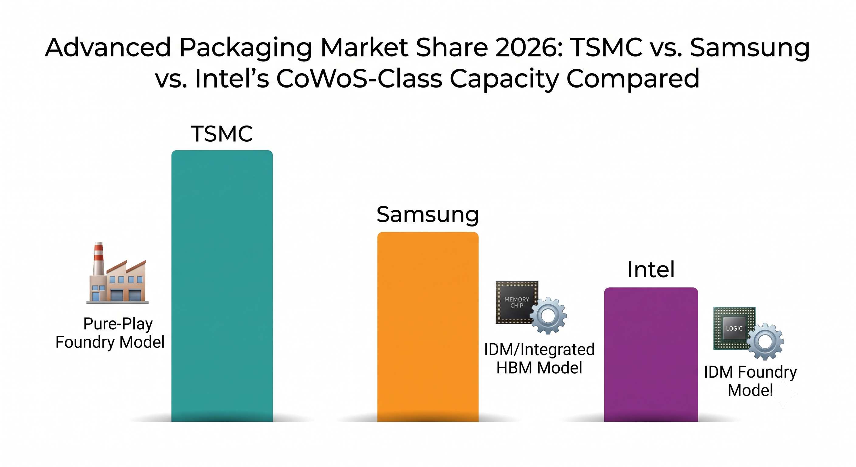
TSMC leads advanced packaging capacity in 2026, with roughly 120,000-140,000 CoWoS wafers per month targeted at TSMC alone by year-end (and ~200,000/month industry-wide once OSAT partners are counted), while Samsung and Intel are racing to close the gap with different playbooks — Samsung bundling HBM manufacturing with its own I-Cube/X-Cube packaging as a "turnkey" pitch, and Intel scaling EMIB and Foveros through a newly built Malaysia complex. None of these three compete on exactly the same terms: TSMC packages other companies' chips as a pure-play foundry, Samsung packages chips it also makes the memory for, and Intel is packaging both its own chips and (increasingly) external customers' as an IDM turning foundry. That distinction matters more than any single capacity number if you're actually trying to figure out where to get chips packaged.
Quick Facts
| Question | Answer |
|---|---|
| Who has the largest pure-play foundry market share in 2026? | TSMC, at roughly 72.3% in Q1 2026 (Samsung ~6.5%), per TrendForce data as reported by Sammy Fans |
| How much CoWoS capacity will TSMC have by end-2026? | TrendForce reports 120,000-140,000 wafers/month at TSMC alone, with total industry capacity (TSMC + OSAT partners) approaching ~200,000 wafers/month |
| Who's buying most of TSMC's CoWoS capacity? | Nvidia reportedly holds roughly 60% of allocated capacity, with Broadcom (~15%) and AMD (~11%) reported as the next-largest customers — treat these as directional estimates, not confirmed disclosures |
| What is Samsung's advanced packaging differentiator? | A turnkey HBM + packaging bundle (I-Cube/X-Cube), including 4µm-pitch hybrid copper bonding Samsung has targeted to enable in 2026 |
| What is Intel's advanced packaging strategy? | Scaling EMIB and Foveros via its new Malaysia "Project Pelican" complex (~$2.7-2.9B in facility-specific capex, reportedly ~99% complete and operational in 2026 — a separate ~$7B/RM30B figure covers Intel's broader multi-phase Malaysia investment since 2021) and larger 120×120mm/12-HBM-stack package formats |
Why "Advanced Packaging Market Share" Isn't One Market
Most coverage of this topic treats TSMC, Samsung, and Intel as if they're competing for the same slice of the same pie, and reports a single "advanced packaging market share" number as if it settles the question. It doesn't, because the three companies aren't running the same business.
TSMC's CoWoS is a pure foundry service — customers like Nvidia, AMD, and Broadcom design chips, TSMC fabricates and packages them, and TSMC never touches the memory. Samsung's pitch is the opposite: it wants to sell you HBM and the packaging that combines it with your logic die in one relationship, which only makes sense for customers willing to buy memory from Samsung in the first place. Intel's EMIB and Foveros started as internal packaging technology for Intel's own chips, and are now being opened up to external Intel Foundry customers — so Intel is simultaneously a customer of its own packaging capacity and, increasingly, a competitor to TSMC and the OSATs (outsourced assembly and test vendors like Amkor and ASE) for other companies' business.
That's also why broad market-research figures that lump TSMC, Samsung, Intel, and pure OSAT vendors into a single "advanced packaging market" total ($X billion today, growing to $Y billion by 2031, at Z% CAGR) are hard to use for a real decision. Those totals are measuring different business models with different revenue-recognition logic — a foundry's packaging revenue and an OSAT's assembly-and-test revenue aren't counted the same way, and neither is directly comparable to CoWoS-specific wafer counts. We've left that broader market-sizing figure out of this piece for that reason; if you're evaluating packaging partners, the capacity and customer-allocation numbers below are the more useful lens.
TSMC's CoWoS Capacity: The Numbers, and Why They Don't All Line Up
TSMC's own capacity signal for CoWoS, per TrendForce's June 2026 reporting, is 120,000-140,000 wafers per month at TSMC alone by the end of 2026, with total industry capacity — TSMC plus OSAT partners doing overflow work — approaching roughly 200,000 wafers per month. TrendForce frames this expansion as the reason the supply-demand gap for CoWoS is narrowing, from around 20% short of demand to a projected ~10% by end-2026.
You may also come across a different set of numbers circulating in financial-media coverage: roughly 675,000 wafers in 2025, climbing to 1,275,000 in 2026, and 2,310,000 in 2027, attributed to Goldman Sachs research. These aren't a contradiction of the monthly TrendForce figures above — they're annual totals rather than year-end monthly rates, and the pattern checks out: dividing each annual figure by 12 gives an average monthly pace of roughly 56,000 (2025), 106,000 (2026), and 193,000 (2027) — all below the corresponding year-end monthly targets (75,000; 120,000-140,000; 200,000+) TrendForce reports, which is exactly what you'd expect from capacity that ramps up over the course of each year rather than starting the year already at its year-end level. Goldman Sachs' own methodology for the annual figure isn't public, and it isn't confirmed whether it's TSMC-only or industry-wide, so treat it as a directionally consistent cross-check rather than a number to combine directly with TrendForce's monthly figure. For capacity comparisons, the monthly, TSMC-scoped TrendForce figure remains the more defensible number to use.
Even with that expansion, TrendForce and other industry reporting continue to describe CoWoS allocation — not raw silicon wafer starts — as the tighter constraint on AI accelerator supply through 2026. In practice, the ceiling on how many finished AI chips can ship in a given quarter is often set by how much CoWoS capacity is available, not by how many logic dies TSMC can etch.
Who's Actually Buying TSMC's CoWoS Capacity
Nvidia is reported to hold the largest share of TSMC's allocated CoWoS capacity. A Morgan Stanley research note — summarized by financial-news outlet Longbridge and broadly corroborated by other industry trackers — puts global 2026 CoWoS demand at roughly 1 million wafers, with Nvidia booking approximately 595,000 wafers (about 60%), Broadcom approximately 150,000 wafers (about 15%), and AMD approximately 105,000 wafers (about 11%). Together, the three account for roughly 86% of global CoWoS demand. None of these figures are numbers TSMC has confirmed itself; they're analyst estimates that vary somewhat by source and by which quarter's bookings are being described, so treat them as directional rather than exact.
What this means practically: if you're a smaller AI chip designer trying to secure CoWoS capacity in 2026, you're not just competing against TSMC's total wafer count — you're competing for the roughly 14% of capacity not already claimed by the three largest customers.
Samsung's Turnkey Play: I-Cube, X-Cube, and Hybrid Copper Bonding
Samsung's advanced packaging strategy leans on a bundle TSMC structurally can't offer: HBM manufacturing and 2.5D/3D packaging from the same company. Samsung markets this as I-Cube (its interposer-based 2.5D platform, roughly comparable in role to CoWoS) and X-Cube (its 3D stacking platform for combining logic and memory more tightly). Per Samsung Semiconductor's own technology blog, the company has targeted enabling 4µm-pitch hybrid copper bonding — a finer, bump-less interconnect pitch than conventional microbump approaches — within X-Cube in 2026. Given how often advanced-packaging timelines slip industry-wide, it's worth checking Samsung's latest disclosures before treating that date as locked in.
The pitch to customers is fewer vendor relationships and (in theory) tighter co-optimization between memory and packaging design. The tradeoff is that it only works for customers already sourcing HBM from Samsung, which narrows the addressable customer base compared to TSMC's foundry-agnostic model.
Intel's Catch-Up Bet: EMIB, Foveros, and Project Pelican
Intel's advanced packaging technologies — EMIB (Embedded Multi-die Interconnect Bridge, for 2.5D side-by-side die placement) and Foveros (for 3D die stacking) — predate the current AI packaging boom, originally built for Intel's own CPU and GPU lines. Intel is now scaling both for external Intel Foundry customers as well as its own products.
The centerpiece of that scale-up is a new Malaysia packaging complex, internally referred to as "Project Pelican." Its packaging-specific capital expenditure is reported at roughly RM12 billion (about $2.7-2.9 billion) — not the larger $7 billion (RM30 billion) figure sometimes attached to it, which actually refers to Intel's broader, multi-phase Malaysia investment commitment announced back in 2021, covering assembly-test and die-prep expansion beyond just the Pelican packaging facility; the two shouldn't be conflated. On completion status: Malaysian Prime Minister Anwar Ibrahim said in December 2025, after meeting Intel CEO Lip-Bu Tan, that the facility was about 99% complete, with a further RM860 million (about $200 million) of investment announced to finish it — a figure TrendForce's March 2026 reporting corroborates in the same dollar terms. Neither the RM12 billion facility cost nor the 99%-complete figure comes from an Intel newsroom release or investor filing; both trace to the Malaysian government's public statements as relayed by regional tech press and TrendForce, which is more authoritative than generic trade-press speculation but still short of an Intel primary disclosure. Alongside the Malaysia buildout, Intel and industry coverage (including Tom's Hardware's reporting on EMIB-T) describe larger package formats — 120×120mm packages supporting 12 HBM stacks today, with a roadmap toward 120×180mm packages supporting 24 HBM stacks reportedly targeted by 2028 — as part of Intel's push to match or exceed the scale of TSMC's largest CoWoS-L configurations.
TSMC vs. Samsung vs. Intel: Side-by-Side Comparison
| Aspect | TSMC (CoWoS) | Samsung (I-Cube / X-Cube) | Intel (EMIB / Foveros) |
|---|---|---|---|
| Business model | Pure-play foundry — packages other companies' chips, doesn't make memory | IDM — bundles its own HBM with its own packaging | IDM turning foundry — packages its own chips and, increasingly, external customers' |
| 2026 capacity signal | 120,000-140,000 wafers/month (TSMC-only, TrendForce), ~200,000/month industry-wide with OSAT partners | Not separately disclosed at comparable wafer-level granularity in current reporting | New Malaysia "Project Pelican" complex (~$2.7-2.9B facility-specific capex, ~99% complete; a separate ~$7B figure covers Intel's broader Malaysia investment since 2021), reportedly operational in 2026 |
| Headline differentiator | Foundry-agnostic — works with any chip designer's logic and memory choices | Turnkey HBM + packaging from one vendor; targeting 4µm-pitch hybrid copper bonding in 2026 | Larger package formats (120×120mm/12 HBM stacks now, roadmap to 120×180mm/24 stacks by 2028) |
| Reported pure-play foundry market share (Q1 2026) | ~72.3% (TrendForce, via Sammy Fans) | ~6.5% (TrendForce, via Sammy Fans) | Not reported in the same pure-play foundry category (IDM model) |
| Primary customer base | Nvidia (reportedly ~60%/595,000 wafers of 2026 CoWoS demand, per Morgan Stanley via Longbridge), Broadcom (~15%/150,000 wafers), AMD (~11%/105,000 wafers) — directional analyst estimates, ~14% residual for other customers | Customers already sourcing HBM from Samsung | Intel's own product lines, plus early external Intel Foundry customers |
What This Means If You're Actually Buying Packaging Capacity
If you're a chip designer or procurement lead evaluating where to get advanced packaging done in 2026, the honest framing is: TSMC has the largest and best-utilized capacity, but a meaningful share of it is already spoken for by three customers. Samsung's turnkey bundle is worth evaluating specifically if you're already sourcing HBM from Samsung or want a single vendor relationship for memory-plus-packaging — not as a general CoWoS alternative. Intel's EMIB/Foveros capacity is the newest and least proven at scale for external customers, but its larger package formats and newly built Malaysia capacity make it worth tracking as a second-source option, particularly for designs that need more than 12 HBM stacks in a single package.
None of this is a stock-picking exercise — it's a supply-chain question. If your product roadmap depends on advanced packaging capacity in 2026-2027, the constraint to plan around is allocation timing and vendor lock-in risk, not just which company reports the biggest wafer number this quarter.
For the underlying packaging technology itself — how CoWoS and hybrid bonding actually work, rather than who has the most of it — see our companion explainer, CoWoS and Hybrid Bonding Explained. For where substrate materials are headed next as these packages get larger and hotter, see Glass Core Substrate Explained.
FAQ
Q: Who has the biggest CoWoS-class packaging capacity, TSMC or Samsung?
A: TSMC, by a wide margin, on wafer-level capacity — TrendForce reports TSMC targeting 120,000-140,000 CoWoS wafers per month by end-2026. Samsung doesn't disclose comparable wafer-level figures for I-Cube/X-Cube in current reporting; its differentiator is bundling packaging with its own HBM manufacturing rather than competing on raw capacity.
Q: Is Intel's Foveros as advanced as TSMC's CoWoS?
A: They solve overlapping but not identical problems — Foveros is Intel's 3D die-stacking technology and EMIB handles 2.5D side-by-side placement, roughly analogous in role to TSMC's SoIC and CoWoS respectively. Intel's technology is newer at scale for external customers; its reported roadmap toward 120×180mm/24-HBM-stack packages by 2028 is aimed at matching or exceeding TSMC's largest current CoWoS-L configurations, but it's not yet proven at TSMC's production scale.
Q: Why is CoWoS capacity considered a bottleneck for AI chip supply?
A: Because industry reporting describes advanced-packaging allocation, not raw silicon wafer starts, as the binding constraint on how many finished AI accelerators can ship — even as TSMC expands CoWoS capacity sharply, demand led by Nvidia has kept packaging the tighter chokepoint through 2026.
Q: How much of TSMC's CoWoS capacity does Nvidia use?
A: Nvidia is reportedly allocated roughly 60% of TSMC's CoWoS capacity, per a Morgan Stanley analysis widely cited in industry coverage, with Broadcom (~15%) and AMD (~11%) reported as the next-largest customers. These are directional estimates from analyst and aggregator commentary, not figures TSMC has confirmed itself.
Q: What's the difference between CoWoS, I-Cube/X-Cube, and EMIB/Foveros?
A: They're each a vendor's own name for a similar underlying idea — combining a logic die with HBM memory in one advanced package — built on different business models. CoWoS is TSMC's foundry-agnostic 2.5D/3D platform; I-Cube/X-Cube is Samsung's version, sold as a bundle with Samsung-made HBM; EMIB/Foveros is Intel's version, built first for Intel's own chips and now being extended to external Intel Foundry customers.
Sources
- TrendForce, "TSMC CoWoS Supply-Demand Gap Reportedly Seen Narrowing from 20% to 10% by End-2026 as Capacity Expands" (June 2026)
- TrendForce, "Intel Ramps Up Advanced Packaging: Malaysia Complex Operational in 2026, EMIB Update" (March 2026)
- Samsung Semiconductor Global tech blog, "Advanced Packaging and the Shift to System-Level Semiconductor Innovation"
- SemiWiki, Samsung X-Cube (Extended Cube) industry wiki page
- Tom's Hardware, "Intel's EMIB-T heads for fab rollout this year"
- Sammy Fans, coverage of TrendForce Q1 2026 Samsung/TSMC foundry business data — TSMC 72.3%, Samsung 6.5% (June 2026)
- Morgan Stanley analysis of Nvidia's CoWoS capacity booking (~60% share), as cited in industry coverage of TSMC's advanced-packaging allocation
- Longbridge, "Morgan Stanley elaborates on TSMC's CoWoS capacity battle: NVIDIA secures 60%, cloud AI chip market expected to surge 40%-50% by 2026" — Nvidia 595,000 wafers, Broadcom 150,000 wafers (~15%), AMD 105,000 wafers (~11%) of ~1M global 2026 CoWoS demand
- io-Fund, "Intel vs TSMC: How CoWoS Packaging Constraints Could Create an Opportunity for Intel Foundry" — cites Goldman Sachs annual CoWoS capacity figures (675,000 wafers 2025, 1.275M 2026, 2.31M 2027)
- TechWireAsia, "Intel pours RM860m investment into Malaysia as Penang facility nears done" — Malaysian PM Anwar Ibrahim's Dec. 2025 statement on Project Pelican's ~99% completion and RM12B facility capex (December 2025)
Author Bio
The Whitepaper Skeptic has direct project experience in semiconductor packaging strategy, including advanced packaging materials work on a Corning-related project, and has continued tracking TSMC's CoWoS capacity build-out and its competitors' packaging roadmaps as part of ongoing AI hardware supply-chain analysis.
Related Posts
- What Is HBM (High Bandwidth Memory)? A Beginner's Guide to AI Chip Packaging
- CoWoS and Hybrid Bonding Explained: TSMC's Advanced Packaging Behind AI Chips
- Glass Core Substrate Explained: Why Intel and TSMC Are Replacing Organic Chip Packaging (2026-2028 Timeline)
- HBM4E Explained: What Changes When Custom Base Dies Arrive in 2027-2028
- HBM Burn-In and Known-Good-Die Testing Explained: Why Memory Testing Moved Left


Comments
Post a Comment