Co-Packaged Optics Explained: How Silicon Photonics Cuts AI Data Center Power 3.5x in 2026
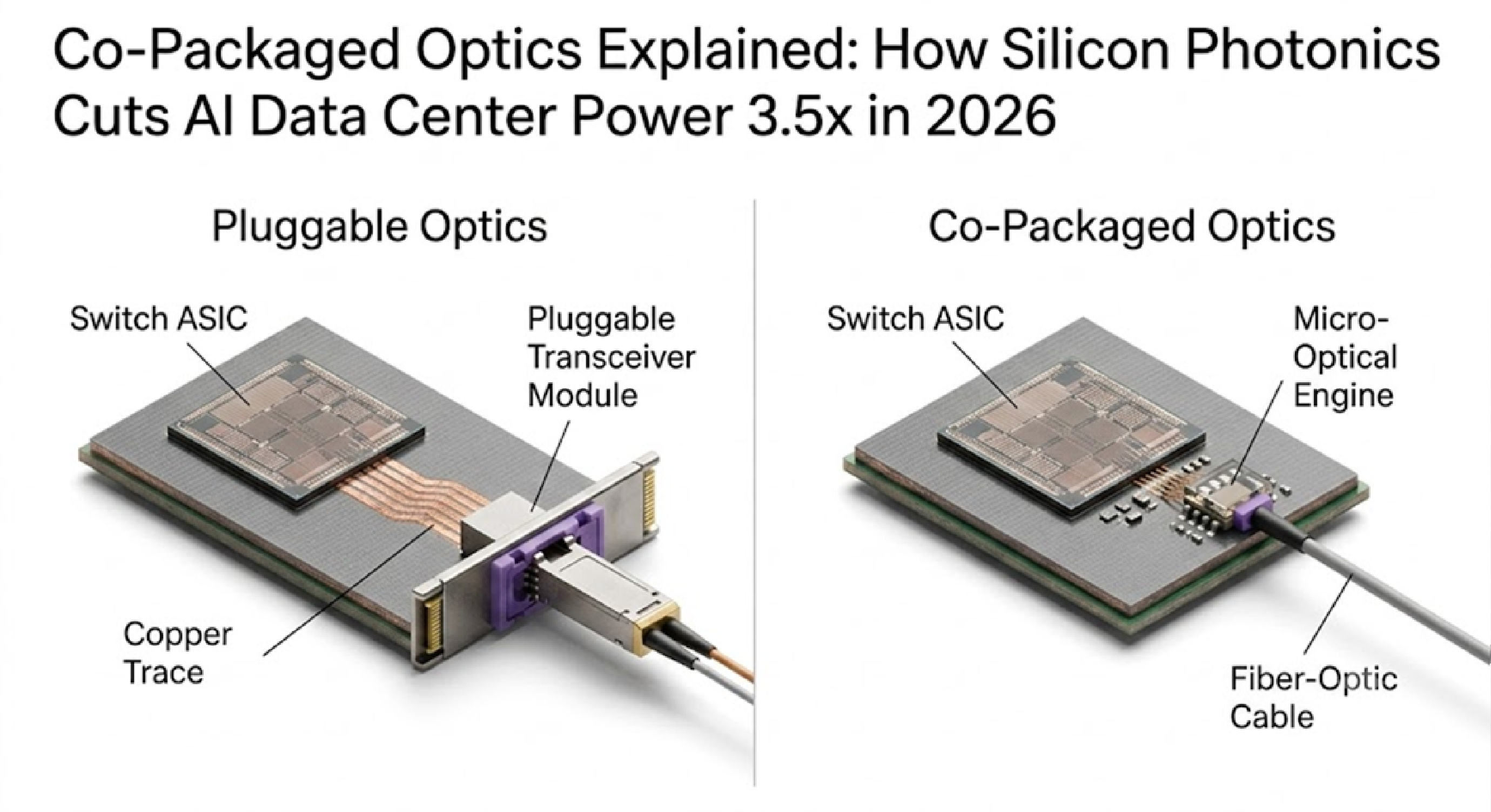
Co-packaged optics (CPO) is a switch design that solders the optical-to-electrical conversion hardware — the "optical engine" — directly onto the same package as the switch ASIC, replacing the pluggable transceiver modules that today plug into the front panel. By shortening the electrical path between the switch chip and the light source, CPO cuts power consumption and signal loss sharply enough that Nvidia claims roughly 3.5x lower power than pluggable optics for the same switching capacity (Nvidia's own figures put pluggable transceivers at roughly 30 W per interface versus about 9 W for CPO). In 2026, CPO moved from lab demonstration to volume shipping for the first time, led by TSMC's COUPE packaging platform, Nvidia's Quantum-X and Spectrum-X Photonics switches, and Broadcom's Bailly and Tomahawk 6 switches. This article explains what CPO actually is, how it compares to pluggable optics, who is shipping it in 2026, and why the real constraint on scaling it up is packaging capacity — not the photonics design itself.
Quick Facts
| Question | Answer |
|---|---|
| What is co-packaged optics? | Optical engines soldered directly onto the switch package instead of plugging in as separate front-panel transceiver modules — shortens the electrical path between switch ASIC and light source |
| What changed in 2026? | TSMC's COUPE silicon photonics platform is on track for mass production in 2026, and both Nvidia (Quantum-X/Spectrum-X Photonics) and Broadcom (Bailly, Tomahawk 6 "Davisson") began shipping CPO switches at volume |
| How much power does it save? | Nvidia claims roughly 3.5x lower power and a signal-loss reduction from 22 dB to 4 dB versus pluggable optics — a vendor-sourced figure, not yet independently benchmarked |
| What's the real bottleneck? | TrendForce reports optical engine yield and advanced-packaging capacity — not the photonics design — as the binding constraint on how fast Nvidia and Broadcom can ramp volume in 2026 |
| Who's behind on CPO? | Samsung is targeting CPO turnkey manufacturing only by 2029, a multi-year lag behind TSMC's 2026 COUPE ramp |
What Is Co-Packaged Optics, and Why It's the Next Advanced-Packaging Bottleneck
Every high-bandwidth switch needs to convert electrical signals into light for transmission over fiber, and back into electrical signals on the receiving end. Today, that conversion happens in pluggable transceiver modules — small hot-swappable units that plug into the front panel of the switch and connect to the switch ASIC over several centimeters of copper trace. That copper trace is the problem: at the data rates modern AI clusters need, driving a signal that far electrically burns a large amount of power and degrades signal integrity before the light conversion even happens.
Co-packaged optics moves the optical engine — the component that does the electrical-to-optical conversion — off the front panel and onto the same package substrate as the switch ASIC itself, next to the compute die rather than several centimeters away. Shortening that electrical path is the entire mechanism behind CPO's power and signal-loss gains; it's a packaging decision as much as a photonics one.
That framing matters for readers of our HBM explainer: CPO isn't best understood as a networking upgrade in isolation. It's the next stage of the same advanced-packaging capacity story that has already reshaped how AI chips are built. TSMC's COUPE (Compact Universal Photonic Engine) silicon photonics platform is explicitly positioned by TSMC as a packaging platform adjacent to CoWoS — the same wafer-and-substrate packaging family we cover in our CoWoS and hybrid bonding explainer. In other words, the company that packages your HBM stacks onto a GPU is the same company packaging the optical engines onto next-generation AI switches, using overlapping fab capacity and expertise.
Co-Packaged Optics vs. Pluggable Optics
| Property | Pluggable optics (today's standard) | Co-packaged optics (CPO) |
|---|---|---|
| Optical engine location | Front-panel module, connected to switch ASIC by several centimeters of copper trace | Soldered directly onto the switch package, next to the ASIC |
| Power consumption | Higher — electrical signal must be driven a longer distance before conversion | Roughly 3.5x lower per Nvidia's claim, from the shorter electrical path |
| Signal loss | Higher — Nvidia cites approximately 22 dB of loss for pluggable optics in its comparison | Lower — Nvidia cites approximately 4 dB for its CPO switches |
| Serviceability | Hot-swappable — a failed transceiver can be replaced without touching the switch | Not hot-swappable — the optical engine is part of the package, so a failure is harder to service in the field |
| Manufacturing maturity (2026) | Mature, industry-standard, high-volume supply chain | Volume ramp just beginning in 2026, constrained by optical engine yield and packaging capacity |
| Best fit | General-purpose networking, smaller clusters, easier field replacement | Largest AI training/inference clusters where power density and bandwidth per switch matter more than field serviceability |
The serviceability tradeoff is worth being explicit about: CPO isn't a strictly better version of pluggable optics, it's a different point on the power/bandwidth-versus-serviceability curve. That's why 2026 deployments are concentrated in the highest-scale AI factory clusters, where the power and signal-loss gains are worth the loss of hot-swap repairability, rather than replacing pluggable optics everywhere at once.
Who's Shipping Co-Packaged Optics in 2026: TSMC, Nvidia, Broadcom, Samsung
| Company / product | 2026 status | Key specs |
|---|---|---|
| TSMC COUPE (packaging platform) | On track for mass production in 2026, per TSMC and TrendForce reporting | Silicon photonics packaging platform underlying the Nvidia and Broadcom switches below |
| Nvidia Quantum-X Photonics | Early 2026 availability | 144 ports x 800 Gb/s = 115 Tb/s aggregate switch capacity, built on TSMC COUPE optical engines |
| Nvidia Spectrum-X Ethernet Photonics | H2 2026 availability | Up to 409.6 Tb/s aggregate switch capacity (512 ports x 800 Gb/s) |
| Broadcom Bailly (51.2T) | In volume manufacturing with partners Delta Electronics and Micas Networks | 51.2 Tbps switch |
| Broadcom Tomahawk 6 "Davisson" | Began shipping October 2025, built on TSMC COUPE optical-engine technology | 102.4 Tbps, 200 Gb/s per lane, 16x 6.4T Davisson DR optical engines |
| Samsung (CPO turnkey manufacturing) | Targeting 2029 — a multi-year lag behind TSMC | No 2026 volume CPO offering |
As of late July 2026, TrendForce reports that Nvidia and Broadcom are both in volume ramp, but flags optical engine yield and advanced-packaging capacity — not the underlying photonics design — as the binding bottlenecks on how fast that ramp can scale. That distinction matters: the hard part of CPO in 2026 isn't proving the technology works, it's building enough qualified packaging capacity to solder optical engines onto switch packages at volume without tanking yield — the same category of constraint that has already shaped HBM and CoWoS supply in our advanced packaging market share coverage.
Read alongside our glass core substrate explainer, a pattern emerges: TSMC is consistently the first mover across multiple next-generation packaging technologies — glass core substrates, CoWoS-class capacity, and now CPO — while Samsung's timelines across all three trail by roughly two to three years.
Optical (CPO) vs. Electrical (UCIe) Interconnect: Don't Confuse These Two
CPO and UCIe solve related but distinct problems, and it's easy to conflate them because both are "next-generation chip interconnect" stories. UCIe (Universal Chiplet Interconnect Express), covered in our UCIe explainer, is an electrical standard for connecting chiplets inside the same package — die-to-die communication measured in millimeters. Co-packaged optics solves a different-scale problem: module-to-module and rack-to-rack communication over fiber, measured in meters to kilometers, where electrical signaling simply can't reach without unacceptable loss.
Put simply: UCIe is about chiplets talking to each other inside one package. CPO is about switches and GPU clusters talking to each other across a data center. Both are responses to the same underlying pressure — AI workloads outgrowing what a single die, or a single rack, can do alone — but they operate at completely different physical scales and neither one replaces the other.
Does HBM Need Co-Packaged Optics?
Not directly. HBM stacks communicate with the GPU or accelerator die they sit next to using short, high-bandwidth electrical interconnects inside the same package — the interconnect problem our HBM pillar and CoWoS explainer cover. CPO operates one level up the stack, at the switch and rack-to-rack networking layer connecting GPU clusters together, not at the memory-to-compute layer inside a single package. The connection between the two stories is indirect but real: both HBM stacking and CPO switches are downstream of the same AI accelerator power-density and packaging-capacity pressures, and both increasingly depend on TSMC's advanced-packaging fabs rather than purely on chip design.
Where CPO Fits in the AI Data Center Power Story
The 3.5x power reduction CPO promises doesn't exist in a vacuum — it's part of the same power-density crunch reshaping AI data center design broadly. Nvidia's Quantum-X Photonics chassis, like the GPUs it connects, is liquid-cooled, tracing back to the same GPU and switch power density trend we cover in our AI data center liquid cooling explainer. As AI clusters scale toward hundreds of thousands or millions of GPUs, the power spent moving data between switches becomes a meaningful fraction of total cluster power — which is why Nvidia frames CPO explicitly as infrastructure for scaling "AI factories" rather than a routine networking refresh.
The reliability question that comes with volume ramp is closely related to memory testing challenges elsewhere in the packaging stack — see our HBM burn-in and known-good-die testing explainer for how the industry screens for defects before committing expensive packaged components to a rack.
FAQ
Q: What is co-packaged optics (CPO)?
A: Co-packaged optics is a switch design that mounts the optical engine — the component that converts electrical signals to light — directly onto the switch chip's package, instead of housing it in a separate pluggable transceiver module on the front panel. Shortening that electrical path is what drives CPO's power and signal-loss advantages.
Q: How is co-packaged optics different from pluggable optics?
A: Pluggable optics uses hot-swappable front-panel modules connected to the switch ASIC by several centimeters of copper trace. CPO solders the optical engine onto the same package as the switch ASIC, cutting that electrical distance dramatically — Nvidia claims roughly 3.5x lower power and a signal-loss reduction from about 22 dB to 4 dB, though this is a vendor-sourced comparison. The tradeoff is that CPO modules aren't field-serviceable the way pluggable transceivers are.
Q: What is TSMC COUPE?
A: TSMC COUPE (Compact Universal Photonic Engine) is TSMC's silicon photonics packaging platform, positioned as adjacent to its CoWoS advanced-packaging family. It is on track for mass production in 2026 and underlies the optical engines used in Nvidia's Quantum-X and Spectrum-X Photonics switches and Broadcom's Tomahawk 6 "Davisson" switch.
Q: Does HBM need co-packaged optics?
A: No — not directly. HBM communicates with the GPU die next to it over short electrical interconnects inside the same package, which is a separate technology from CPO's switch-to-switch optical networking. The two are related only in that both depend on the same TSMC advanced-packaging capacity and both trace back to the same AI accelerator power-density pressures.
Q: When will co-packaged optics be mass produced?
A: TSMC's COUPE platform is on track for mass production in 2026, and Nvidia and Broadcom both began volume shipping CPO switches during 2026. However, TrendForce reports that optical engine yield and advanced-packaging capacity — not the photonics design itself — remain the binding bottlenecks on how quickly that volume can scale through the rest of 2026 and beyond. Samsung, by contrast, isn't targeting CPO turnkey manufacturing until 2029.
Sources
- Nvidia Newsroom — NVIDIA Announces Spectrum-X Photonics, Co-Packaged Optics Networking Switches to Scale AI Factories to Millions of GPUs
- TrendForce — NVIDIA and Broadcom Begin Volume Ramp of CPO Switches, with Optical Engine Yield and Advanced Packaging Capacity Emerging as Key Expansion Bottlenecks (2026-07-27)
- TrendForce — Silicon Photonics Race Intensifies as TSMC Targets 2026 COUPE Production, Samsung Eyes 2029 CPO Turnkey (2026-04-01)
- EDN — Where co-packaged optics (CPO) technology stands in 2026
- Tom's Hardware — Nvidia outlines plans for using light for communication between AI GPUs by 2026
Author Bio
The Whitepaper Skeptic has direct project experience in semiconductor packaging strategy, including advanced packaging materials work on a Corning-related project, and continues tracking how TSMC's packaging roadmap — from CoWoS to glass substrates to now silicon photonics — shapes capacity and yield constraints across the AI hardware supply chain.
Related Posts
- What Is HBM (High Bandwidth Memory)? A Beginner's Guide to AI Chip Packaging
- CoWoS and Hybrid Bonding Explained
- UCIe Explained: The Open Standard Making Mix-and-Match Chiplets Possible
- AI Data Center Liquid Cooling: Why HBM and GPU Power Density Broke Air Cooling
- Glass Core Substrate Explained: Why Intel and TSMC Are Replacing Organic Chip Packaging (2026-2028 Timeline)
- Who's Winning Advanced Packaging? TSMC, Samsung, and Intel's CoWoS-Class Capacity Compared
- HBM Burn-In and Known-Good-Die Testing Explained: Why Memory Testing Moved Left
Tags
co-packaged optics, silicon photonics, AI data center networking, TSMC COUPE, advanced packaging


Comments
Post a Comment