Intel EMIB Explained: Why SK Hynix Is Testing It as a CoWoS Alternative for HBM Packaging in 2026
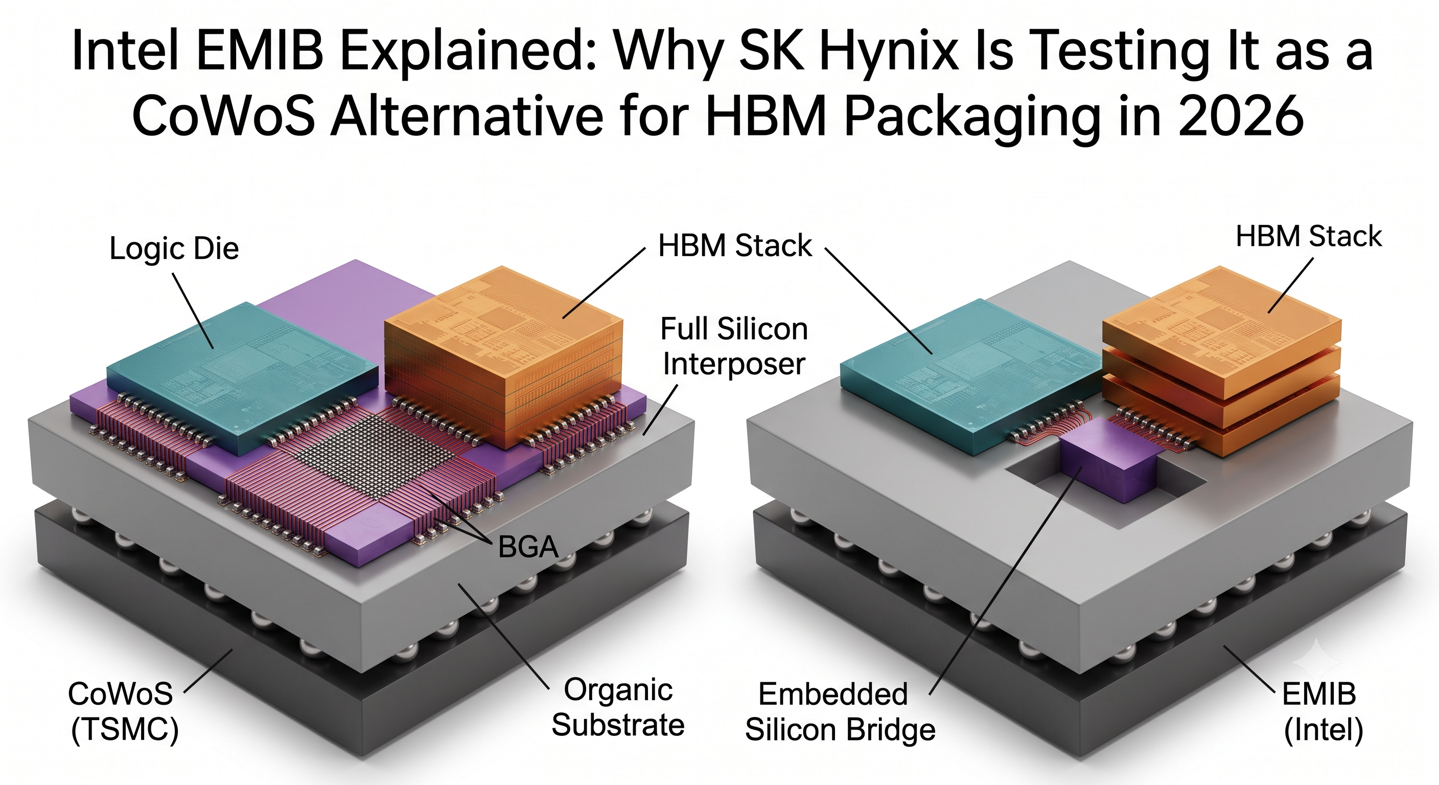
Intel EMIB (Embedded Multi-die Interconnect Bridge) is a 2.5D chip-packaging technology that embeds a small silicon bridge directly into an organic substrate to connect two or more dies side by side — instead of placing every die on top of one large silicon interposer, the way TSMC's CoWoS does. SK Hynix is reportedly testing EMIB as a second HBM-packaging option, on a small-scale domestic R&D line rather than in committed mass production, as persistent capacity tightness in TSMC's CoWoS platform collides with surging AI accelerator demand. Removing the full interposer reportedly improves yield and cuts warpage risk from thermal-expansion mismatch, but it comes at the cost of lower interconnect bandwidth than CoWoS offers — which is why EMIB is currently framed as a better fit for ASIC-class accelerators than for bandwidth-maximizing GPU designs.
By The Whitepaper Skeptic — semiconductor packaging strategy experience, Corning advanced packaging project
Quick Facts
| Question | Answer |
|---|---|
| What is Intel EMIB? | A 2.5D packaging method that embeds a small silicon bridge into the organic substrate to connect dies side by side, avoiding a full silicon interposer |
| How is it different from CoWoS? | CoWoS places dies on top of one large silicon interposer that carries every die-to-die connection; EMIB only puts silicon bridges where die-to-die connections actually need it |
| Why is SK Hynix testing it? | Reportedly as a hedge against TSMC CoWoS capacity tightness amid surging AI accelerator/HBM demand — described as small-scale R&D testing, not a confirmed production switch (TrendForce, May 2026) |
| What's the tradeoff vs. CoWoS? | Reportedly better yield and lower warpage risk, but lower interconnect bandwidth and slightly higher latency than a full-size CoWoS interposer |
| Who else reportedly uses/evaluates EMIB? | Google and Meta, for unspecified future accelerator/chip programs — outlets disagree on exact product names (Google TPU v8e vs. a 2027 TPU with MediaTek; Meta MTIA vs. an in-house Meta CPU), and neither company has confirmed it directly |
What Is Intel EMIB, and How Is It Different From CoWoS?
Both EMIB and CoWoS solve the same basic problem — connecting multiple dies (say, a logic die and one or more HBM stacks) closely enough together that they can communicate at very high bandwidth without routing signals through the much slower, lower-density wiring of a standard organic package substrate. They solve it with opposite architectural choices.
TSMC's CoWoS (Chip-on-Wafer-on-Substrate) — which our CoWoS and hybrid bonding explainer covers in depth — places every die in the package on top of one large silicon interposer, a full sheet of silicon with dense wiring layers that carries every die-to-die and die-to-substrate connection. The interposer then sits on the organic substrate underneath it. Because the interposer is silicon, it's expensive and its usable size is capped by the reticle limits of lithography equipment, but it gives every connection in the package access to dense, uniform, high-bandwidth wiring.
EMIB skips the full interposer. Instead, a small piece of silicon — the "bridge" — is embedded directly into a cavity milled into the organic substrate, positioned only underneath the specific spot where two dies need to talk to each other at high bandwidth. Everywhere else, the dies sit directly on the organic substrate using conventional, cheaper wiring. The result is a package that uses expensive, high-density silicon wiring only where it's actually needed, rather than paying for a full sheet of interposer silicon under the entire package footprint.
Why SK Hynix Is Testing EMIB Now: The CoWoS Capacity Crunch
SK Hynix has historically been a TSMC/CoWoS customer for integrating HBM stacks with logic dies in AI accelerator packages. According to TrendForce (May 2026), SK Hynix is reportedly testing Intel's EMIB as an alternative path to package HBM, driven by persistent tightness in TSMC's CoWoS capacity amid surging demand for AI accelerators. Independent confirmation beyond TrendForce comes from SK Hynix's own Hot Chips 2026 presentation: VP of Package Engineering Jaesik Lee walked through a direct comparison of CoWoS-S, CoWoS-L, and EMIB for HBM packaging, framing packaging choice as a factor in how much mechanical and thermal stress an HBM stack has to absorb. That August 2026 talk — which post-dates the May TrendForce report — treats EMIB as one packaging approach under active technical evaluation alongside CoWoS-S/L, consistent with TrendForce's "testing, not committed mass production" framing rather than superseding it; SK Hynix did not disclose yield, bandwidth, or a production timeline for EMIB specifically at the event.
It's worth being precise about what this test does and doesn't mean. SK Hynix testing a competitor's foundry-arm packaging technology is not the same as SK Hynix committing to replace CoWoS. TrendForce's own framing places EMIB as one option among several SK Hynix is evaluating alongside its broader 2026 advanced-packaging diversification — SK Hynix has separately discussed its CoWoS-S/L usage and its own MUST/hybrid-bonding roadmap at Hot Chips 2026. For the market-share and capacity context behind why CoWoS is tight in the first place, see our advanced packaging market share breakdown of TSMC, Samsung, and Intel, which covers Intel's own EMIB/Foveros capacity scale-up numbers in more detail than this article re-derives.
EMIB vs. CoWoS: Yield, Warpage, Bandwidth, and Latency Tradeoffs
The mechanical difference between the two approaches — bridge-only vs. full interposer — drives a specific set of tradeoffs that explain why a memory maker would even consider testing a second-source packaging option in the first place.
| Factor | Intel EMIB | TSMC CoWoS |
|---|---|---|
| Interposer approach | Small silicon bridge embedded in organic substrate, only under die-to-die connection points | Full silicon interposer spans the entire package footprint |
| Reported yield | ~90% as of April 2026, reported by multiple independent trade-press outlets (TrendForce, wccftech, and others), each tracing the figure to GF Securities analyst Jeff Pu rather than an Intel Foundry disclosure — treat as an analyst estimate reported consistently across outlets, not a confirmed Intel number | Yield scales with the interposer's size and the reticle-stitching needed for large multi-die packages; not directly comparable to a single EMIB figure without a matched package-size baseline |
| Warpage risk | Reportedly lower — less full-size silicon interposer means less thermal-expansion mismatch across the package | Higher warpage risk on large, reticle-stitched interposers, a known challenge as CoWoS packages have grown to fit more HBM stacks |
| Interconnect bandwidth | Lower than a full-size CoWoS interposer — bridges only carry the specific connections routed through them | Higher — the full interposer gives every connection dense, uniform high-bandwidth wiring |
| Latency | Reportedly slightly higher than CoWoS | Reportedly lower, given the uniform interposer wiring |
| Best-fit workload (as currently framed) | ASIC-class accelerators (e.g., custom AI chips) where the bandwidth ceiling is an acceptable tradeoff for yield/cost | GPU-class designs that need to maximize interconnect bandwidth across many HBM stacks |
The warpage row is the one I would refuse to accept unqualified. Evaluating advanced packaging materials taught me to send every flatness or warpage claim back with three questions attached — at what body size, on what substrate stack-up, through what reflow profile — because the same material can look comfortable at one package footprint and be unbuildable two steps up. The ~90% yield figure in this table has the same shape of problem: it is a single number, sourced to an analyst rather than an Intel disclosure, with no stated package size behind it. A bridge that deletes the full interposer should warp less than a reticle-stitched one; how much less, at what footprint, is a question nobody in this story has published a matched answer to.
A note on precision: the bandwidth/latency comparisons above are directional, not quantified. Neither Intel Foundry's own EMIB technical materials nor TSMC's 3DFabric documentation publish a matched, apples-to-apples bandwidth-per-mm or GB/s figure for EMIB versus CoWoS at comparable package sizes, and independent industry analyses that attempt a numeric comparison (e.g., pJ/bit power-efficiency estimates) aren't corroborated across multiple sources — so this article sticks to the qualitative "lower bandwidth, slightly higher latency" framing that is consistently reported, rather than citing a specific number that can't be independently confirmed.
Who Else Reportedly Uses EMIB? Google, Meta, and the ASIC Angle
EMIB isn't new — Intel has used it in its own products for years — but its relevance to the HBM-packaging conversation comes from which AI accelerator makers are reportedly adopting or evaluating it. Trade press coverage reports Google and Meta as evaluating or adopting EMIB for future accelerator designs, though outlets don't fully agree on the specifics: TrendForce and several outlets name Google's TPU v8e (reportedly targeting an H2 2027 timeline), while at least one other industry analysis describes the Google program as a 2027 TPU built with MediaTek rather than v8e specifically. Meta's product is similarly described inconsistently — most coverage points to Meta's MTIA accelerator family, while TrendForce's original report instead describes an in-house Meta CPU program targeting H2 2028. None of this has been confirmed directly by Google or Meta in an earnings call, technical disclosure, or other primary source, and the inconsistency across secondary sources on exact product names and timelines is itself a reason for caution — treat all of it as "reportedly," not settled fact.
The pattern, if the reporting holds regardless of which exact product name turns out to be accurate, fits the yield/bandwidth tradeoff described above: Google's and Meta's programs are both custom ASIC-class accelerators (or, per some reports, custom CPUs) built for a specific, known workload rather than general-purpose GPUs that need to maximize bandwidth across every possible AI workload. That makes EMIB's yield and cost advantages a more attractive trade for ASIC/custom-silicon designers than for GPU vendors chasing maximum interconnect bandwidth per package.
Where This Fits: SK Hynix's Broader Packaging Diversification
EMIB testing doesn't happen in isolation — it's one thread in SK Hynix's wider 2026 push to diversify its advanced-packaging options beyond a single-vendor CoWoS dependency, alongside its own MUST/hybrid-bonding roadmap and continued use of CoWoS-S/L. That diversification story sits close to two other threads on this site: the generation-over-generation base-die sourcing choices covered in our custom HBM base die explainer, and the testing/yield side of HBM production covered in our HBM burn-in and known-good-die testing explainer — both 2026 stories about memory makers reducing single points of dependency in the HBM supply chain, just at a different layer than packaging architecture.
FAQ
Q: What is Intel EMIB used for?
A: EMIB (Embedded Multi-die Interconnect Bridge) is a 2.5D packaging technology that connects two or more dies at high bandwidth by embedding a small silicon bridge into the organic substrate beneath the connection point, instead of placing the dies on a full silicon interposer. It's used to link logic dies with memory (including HBM) or other logic dies without the cost and size limits of a full interposer.
Q: Is Intel EMIB the same as CoWoS?
A: No. Both are 2.5D packaging technologies used to connect multiple dies at high bandwidth, but they use opposite architectures: CoWoS (TSMC) places every die on top of one large silicon interposer, while EMIB (Intel) embeds small silicon bridges only under the specific points where dies need a high-bandwidth connection. They're alternative approaches to the same packaging problem, not the same technology under different names.
Q: Why is SK Hynix testing Intel EMIB for HBM?
A: Reportedly to hedge against capacity tightness in TSMC's CoWoS platform, which has been under sustained pressure from surging AI accelerator demand (TrendForce, May 2026). SK Hynix's EMIB testing is described as small-scale domestic 2.5D packaging R&D, not a committed mass-production switch — it's one option in a broader packaging diversification effort that also includes SK Hynix's own MUST/hybrid-bonding roadmap.
Q: Does EMIB have lower bandwidth than CoWoS?
A: Yes, as currently reported — EMIB's bridge-only approach delivers lower interconnect bandwidth and slightly higher latency than CoWoS's full-size interposer, in exchange for reportedly better yield and lower warpage risk. That tradeoff is why EMIB is currently viewed as a better fit for ASIC-class accelerators than for GPU-class designs that need to maximize bandwidth across many HBM stacks.
Q: What is Intel's reported EMIB yield rate?
A: Trade press has cited a roughly 90% yield milestone for Intel EMIB as of April 2026. Multiple independent outlets (TrendForce, wccftech, and others) report the same figure, each attributing it to GF Securities analyst Jeff Pu rather than an Intel Foundry disclosure — treat it as a consistently reported analyst estimate rather than an official Intel number.
Sources
- SK hynix Reportedly Tests Intel EMIB 2.5D Packaging With HBM Amid TSMC CoWoS Tightness — TrendForce (2026-05-11)
- Intel, SK hynix shares surge following reports of chip packaging partnership — Tom's Hardware
- SK Hynix Unpacks Advanced Packaging Technologies, Including Intel EMIB, For Its Next-Gen HBM Memory — wccftech
- SK hynix HBM Packaging at Hot Chips 2026 — ServeTheHome
- SK hynix Considers Using Intel's EMIB 2.5D Packaging for HBM Memory — whatpsu.com
- Intel's U.S. Advanced Packaging Enables Next-Generation AI Semiconductors — Intel Newsroom
- Intel's EMIB Hits 90% Yield as Analyst Signals Foundry Breakthrough — wccftech
Author Bio
The Whitepaper Skeptic has direct project experience in semiconductor packaging strategy, including advanced packaging materials work on a Corning-related project, and has continued tracking how competing 2.5D and 3D packaging architectures — interposers, bridges, and hybrid bonding — trade off yield, cost, and bandwidth as AI accelerator makers diversify their HBM integration supply chains.
Related Posts
- What Is HBM (High Bandwidth Memory)? A Beginner's Guide to AI Chip Packaging
- CoWoS and Hybrid Bonding Explained
- Who's Winning Advanced Packaging? TSMC, Samsung, and Intel's CoWoS-Class Capacity Compared
- Custom HBM Base Die Explained: How TSMC, Samsung, and SK Hynix Are Redesigning HBM4E in 2026
- HBM Burn-In and Known-Good-Die Testing Explained: Why Memory Testing Moved Left


Comments
Post a Comment