EUV Lithography Explained: Why High-NA EUV Is the 2026 Bottleneck for the Next Process Node
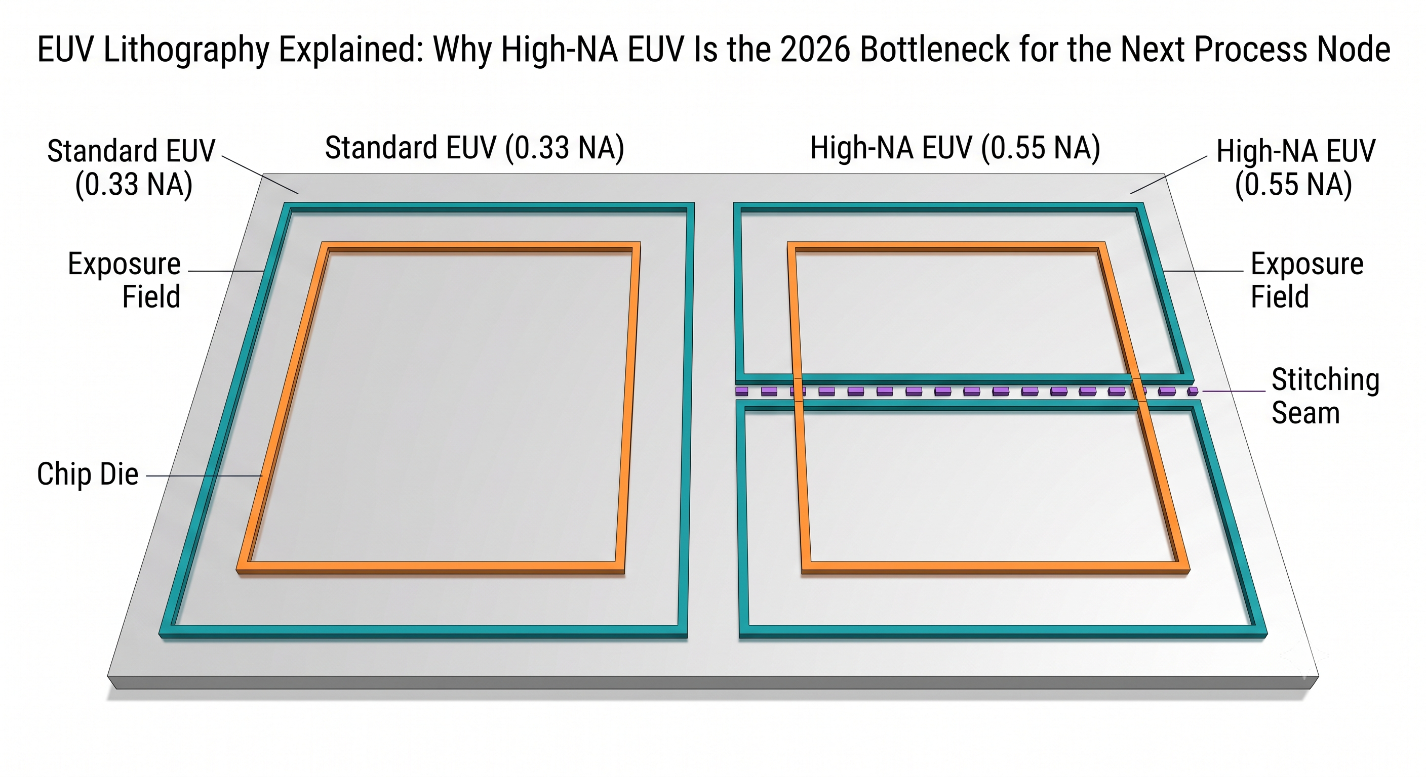
High-NA EUV is the next generation of extreme ultraviolet lithography — ASML's TWINSCAN EXE:5200B — which raises the numerical aperture (NA) of the optics from 0.33 to 0.55 to print sharper, smaller transistor features. The catch is the trade-off nobody puts in the headline: that resolution gain comes from optics that cut the usable exposure field roughly in half, which means large chip designs no longer fit in a single exposure and have to be "stitched" together from two — a real yield and design-rule complication, not a footnote. That trade-off, plus a roughly $400M price tag per scanner, is why Intel is already running limited production on High-NA while TSMC has publicly said "not yet."
By The Whitepaper Skeptic — semiconductor packaging strategy work on a Corning project
Quick Facts
| Question | Answer |
|---|---|
| What is High-NA EUV? | ASML's TWINSCAN EXE:5200B, the next EUV lithography generation, raising numerical aperture from 0.33 to 0.55 with new anamorphic optics from Zeiss |
| How much does one scanner cost? | Roughly $400M per unit (widely cited across trade press; likely a unit price rather than a full total-cost-of-ownership figure) |
| What's the trade-off for the resolution gain? | The exposure field is cut to roughly 26×16.5mm² — about half the standard 0.33 NA full field — which forces large dies to be "stitched" from two exposures |
| Who's running it in production first? | Intel, which has installed the industry's first commercial unit and reports limited High-NA production tied to its 18A-to-14A roadmap |
| Is TSMC using it yet? | No — TSMC has publicly deferred adoption over cost, with reporting pointing to roughly 2028 (its A14 node) rather than an earlier node |
What Actually Changed: NA 0.33 to 0.55
Every EUV scanner works by bouncing 13.5nm-wavelength light off a series of mirrors — there's no lens material transparent enough at that wavelength, so the entire optical path is mirrors, manufactured by Zeiss to tolerances measured in atoms. Numerical aperture describes how wide an angle those mirrors can capture and focus light through; a higher NA means a sharper, higher-resolution image on the wafer, which is what lets a fab print smaller, denser transistor features without adding extra patterning steps.
Standard EUV scanners, the ones running today's leading-edge nodes, use 0.33 NA optics. High-NA jumps to 0.55 NA using new anamorphic optics from Zeiss — mirrors that magnify differently along two axes instead of uniformly, a change ASML and imec have both described as necessary to keep the optical system physically buildable at the larger aperture. The payoff is real: finer resolution means fewer multi-patterning steps are needed to print a given feature size, which is the whole reason chipmakers want it. But anamorphic optics only magnify uniformly in one direction, and that's where the trade-off starts.
The Real Bottleneck: Why Halving the Exposure Field Forces Stitching
This is the part most High-NA coverage glosses over as a marketing footnote, and it shouldn't be. Because the new optics only reduce the image non-uniformly, the maximum area a single High-NA exposure can print — the "exposure field" — shrinks to roughly 26×16.5mm², about half the full field a standard 0.33 NA scanner can cover in one shot, per ASML and imec's own technical descriptions of the EXE platform.
For a small chiplet, that's not a problem — plenty of individual dies fit comfortably inside a half-size field. But large logic dies and large HBM base dies, the kind this site's glass core substrate and custom HBM base die explainers cover, routinely exceed a single High-NA field. Printing a die that large on a High-NA scanner means splitting its layout across two exposures and "stitching" them together at a seam — and that seam has to align with sub-nanometer overlay precision, or the transistors and interconnects that straddle it end up mismatched, timing-skewed, or simply broken.
Academic and industry technical work — including a first experimental stitching study published through SPIE and IEEE research on stitch challenges specifically for large die designs — treats this as a genuine open engineering problem: overlay budget, design-rule accommodation at the stitch boundary, and yield loss concentrated right along that seam. That's fundamentally different from "the new scanner is faster and sharper, so it's simply better." A fab adopting High-NA for a large die has to either redesign that die to respect the smaller field, accept the stitching risk, or hold that particular design back on standard EUV a while longer — three real trade-offs, not one obvious upgrade.
Coming at this from the packaging side, I had the causality backwards for a long time. On advanced packaging materials work for a Corning-related project, maximum die size was something I treated as a back-end constraint — what the substrate, the interposer, and the assembly flow would hold — with lithography priced in as a cost-per-wafer line item rather than a dimensional one. The 26×16.5mm² field is what corrected that. For a large HBM base die, whether a stitch seam exists at all is decided in the fab, months before any package designer sees the part, and no amount of substrate or bonding work downstream recovers a die that had to be printed in two pieces.
Why It Costs $400M: The Zeiss Mirror Bottleneck
The other reason High-NA adoption isn't a straightforward yes is cost, and the cost traces back to a single-source supply chain constraint. Every EUV mirror — standard or High-NA — is manufactured by Zeiss at its Oberkochen, Germany facility, ground and polished to sub-atomic surface tolerances that no other supplier currently matches at production volume. High-NA's anamorphic optics are more complex to manufacture than standard EUV mirrors, and that complexity, layered onto an already singular supply chain, is a meaningful part of why a single EXE:5200B unit runs roughly $400M — a figure repeated across multiple trade outlets, though it's worth treating as a unit price rather than a confirmed total-cost-of-ownership number, since fab-level installation, facilities, and consumables costs are typically reported separately.
Throughput matters here too, not just the sticker price: trade coverage of Intel's acceptance testing — Bits&Chips and SemiWiki both report this independently — puts the EXE:5200B at roughly 175 wafers per hour under standard conditions with 0.7nm overlay accuracy, with Intel targeting further optimization toward 200+ wafers per hour in production use. (An earlier, higher figure of 195+ wafers/hour paired with a 7g wafer-stage acceleration spec traces back to a single lower-tier aggregator site and doesn't appear in ASML's own materials or in Tom's Hardware, Bits&Chips, or SemiWiki reporting, so it's not used here.)
That price point is also why the adoption question isn't really "does High-NA work" — Intel has already answered that by running it — it's "does the resolution gain justify $400M-per-tool now, on this design, given the stitching risk for anything larger than a half-field die." That's an economics-and-engineering call each fab is making independently, and the four biggest customers aren't making it the same way.
Adoption Timeline: Intel vs. Samsung vs. SK Hynix vs. TSMC
| Fab | 2026 posture | Reported target node/timing | Sourcing confidence |
|---|---|---|---|
| Intel | First to install and run High-NA in commercial production | Limited production tied to its 18A-to-14A roadmap | ASML press release + Tom's Hardware installation reporting |
| Samsung | Has installed two EXE:5200B units at its Hwaseong fab (one in 2025, a second in H1 2026) but hasn't moved to production use | Deferred volume adoption to its 1nm-class (A10) node, reportedly around 2030, rather than the 2nm/1.4nm nodes it originally floated | TrendForce, Aug 2026 (updates and confirms the Feb 2026 comparison) |
| SK Hynix | Reportedly receiving units on a timeline similar to Samsung's original (pre-deferral) plan | Not specified in available reporting | TrendForce, Feb 2026 comparison coverage |
| TSMC | Publicly deferred adoption, citing cost | Reportedly ~2028, tied to its A14 node | AnySilicon / trade-press cost-deferral coverage |
What makes this table worth pausing on isn't that one company is "ahead" — it's that the two largest foundries by volume, TSMC and Samsung, are both hedging on a tool Intel has already put into production, even though Samsung has physically installed two of the same EXE:5200B units Intel is running. Owning the scanner and running it in volume production turned out to be two different decisions. For a technology transition this expensive, that's an unusual amount of caution from the market leaders rather than the laggard, and it's a more honest read of the stitching/cost trade-off above than "High-NA is obviously the future and some fabs just haven't caught up yet."
Where This Fits in the HBM and Chiplet Story
Every other spoke in this site's hbm-chiplet cluster so far — glass core substrate, backside power delivery, custom HBM base die, CoWoS and hybrid bonding — covers what happens after a die is already fabricated: how it gets stacked, wired for power, or connected to other dies in a package. This article is the first spoke in the cluster to go a layer further back, into the front-end wafer process that determines the transistor density those packaging techniques are stacking and connecting in the first place.
The connection to the HBM pillar is upstream rather than direct: HBM itself — the DRAM dies, the logic base die discussed in the custom base die piece above — is downstream of the same process-node economics this article explains. Whatever lithography a fab uses (or delays adopting) shapes the transistor density and cost structure of the logic dies that HBM stacks sit next to, even though HBM's own DRAM layers are manufactured on separate, typically less bleeding-edge processes. Meanwhile, the packaging techniques covered elsewhere in this cluster — hybrid bonding, backside power delivery, glass core substrates — operate entirely downstream of whatever comes out of a lithography step like this one; they don't depend on which NA a fab used, but they do depend on the transistor density and die-size constraints that NA choice creates.
FAQ
Q: What is High-NA EUV lithography?
A: High-NA EUV is the next generation of extreme ultraviolet chip lithography, built around ASML's TWINSCAN EXE:5200B scanner. It raises the numerical aperture of the optics from 0.33 to 0.55 using new anamorphic mirrors from Zeiss, which sharpens resolution enough to print smaller transistor features with fewer multi-patterning steps than standard EUV needs.
Q: Why is High-NA EUV so expensive?
A: A single EXE:5200B unit is widely reported to cost roughly $400M, driven largely by the complexity of manufacturing its anamorphic mirrors — all EUV mirrors, standard or High-NA, come from a single supplier, Zeiss, and High-NA's optics are more complex to produce than standard EUV mirrors at an already singular supply chain.
Q: What is EUV stitching, and why does it matter for High-NA?
A: High-NA's anamorphic optics cut the maximum single-exposure field to roughly 26×16.5mm², about half the standard EUV full field. Chip designs larger than that field have to be split across two exposures and aligned ("stitched") at a seam with sub-nanometer overlay precision — a real yield and design-rule risk for large logic dies and large HBM base dies, not just a manufacturing footnote.
Q: When will TSMC start using High-NA EUV?
A: TSMC has publicly deferred High-NA adoption over cost concerns, with reporting pointing to roughly 2028 and its A14 process node rather than an earlier node — well behind Intel, which is already running limited High-NA production in 2026.
Q: Is Samsung using High-NA EUV yet?
A: Not for production. Samsung has installed two EXE:5200B units at its Hwaseong fab — one in 2025, a second in the first half of 2026 — so the equipment is there. But as of mid-2026 reporting, Samsung has deferred moving High-NA into volume production, now targeting its 1nm-class (A10) node around 2030 rather than the 2nm/1.4nm nodes it originally floated, putting it in a similarly cautious position to TSMC.
Sources
- ASML — official press release, "High NA EUV reaches new readiness milestone with first high-volume Logic product"
- imec — "Entering the High NA EUV Lithography era" and "High-NA EUV lithography: the next step after EUVL"
- Tom's Hardware — "Intel installs industry's first commercial High-NA EUV lithography tool"
- TrendForce — "ASML's High-NA EUV for 2027-28: Which Giants Are Betting Big—Intel, Samsung, SK hynix or TSMC?" (Feb 2026)
- TrendForce — "Samsung Reportedly Eyes High-NA EUV for 1nm around 2030 as TSMC Also Takes a Cautious Approach" (Aug 2026)
- SPIE Digital Library — "Stitching at high-NA EUV: a first experimental study" and IEEE — "Optimizing and Addressing Stitch Challenges in High-NA EUV Lithography for Large Die Designs"
- AnySilicon — "ASML Expects First High-NA EUV Chips Within Months as TSMC Delays Adoption Over Cost Concerns"
- Bits&Chips — "ASML ships first high-NA EUV production scanner" and SemiWiki — "Intel and TSMC Take Different Paths to High-NA EUV" — independent corroboration for the Intel installation and throughput reporting
Author Bio
The Whitepaper Skeptic has direct project experience in semiconductor packaging strategy, including advanced packaging materials work on a Corning-related project, and tracks front-end process-node economics — including EUV and High-NA adoption timing across the major foundries — as part of ongoing AI hardware supply-chain analysis, with particular attention to where wafer-level lithography constraints intersect with the back-end packaging decisions covered elsewhere on this site.
Related Posts
- What Is HBM (High Bandwidth Memory)? A Beginner's Guide to AI Chip Packaging
- Glass Core Substrate Explained: Why Intel and TSMC Are Replacing Organic Chip Packaging
- Backside Power Delivery Explained: How Intel's PowerVia and TSMC's Super Power Rail Are Rewiring Chip Power in 2026
- Custom HBM Base Die Explained: How TSMC, Samsung, and SK Hynix Are Redesigning HBM4E in 2026
- CoWoS and Hybrid Bonding Explained


Comments
Post a Comment