Micro-LED Mass Transfer Explained: Why the Industry Needs "Six Nines" Yield to Beat OLED in 2026
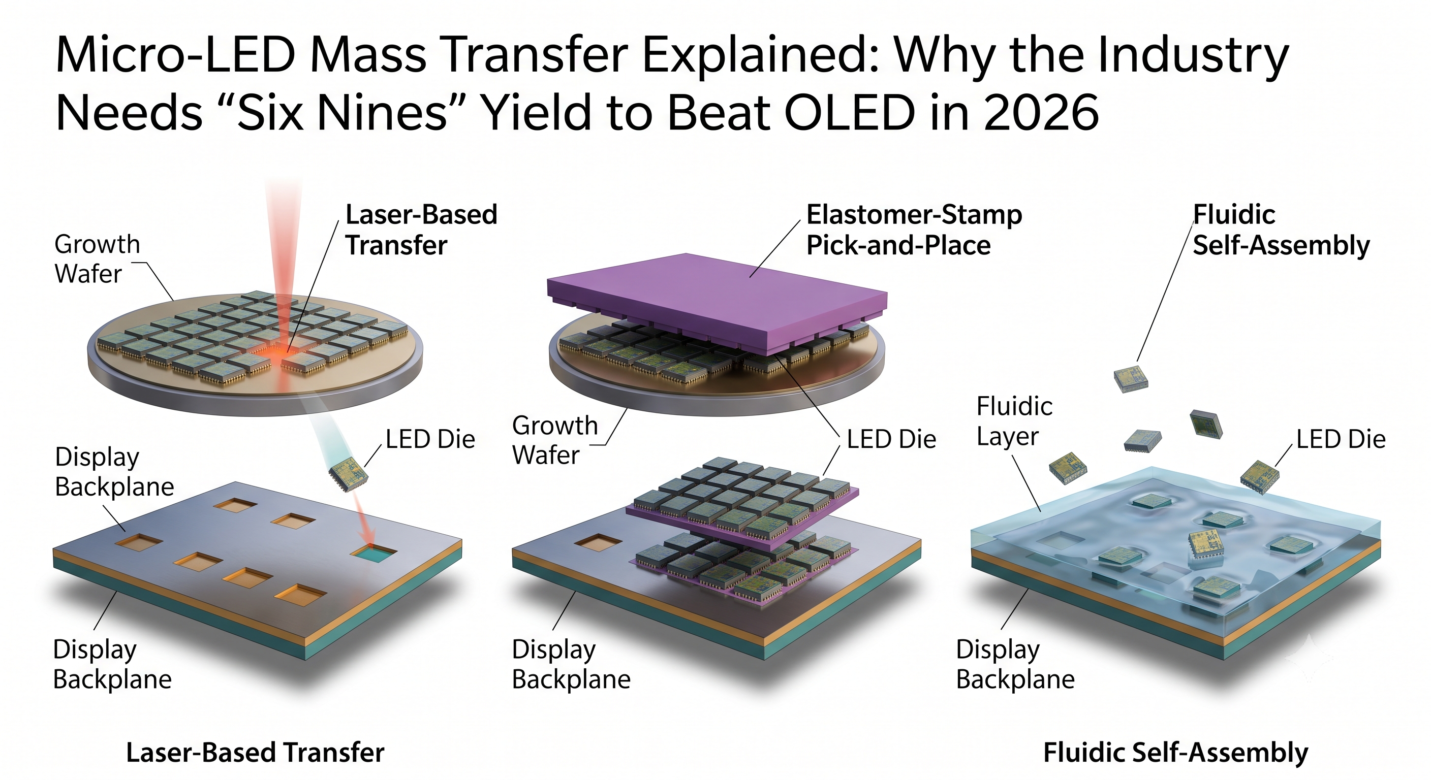
Mass transfer is the manufacturing step that moves millions of microscopic LED die from a growth wafer onto a display backplane, and it remains microLED's central unsolved manufacturing problem in 2026. Three competing technology families — laser-based transfer, elastomer-stamp pick-and-place, and fluidic self-assembly — are racing to hit "six nines" (99.9999%) transfer yield, the widely cited bar for commercial viability, and even the best 2026 pilot lines are reported to still be roughly two orders of magnitude short of it. That yield gap — not brightness, contrast, or lifetime — is the direct reason microLED remains confined to large-format and high-price applications instead of reaching phones or affordable TVs.
By The Whitepaper Skeptic — display materials qualification + process-yield economics experience
Quick Facts
| Question | Answer |
|---|---|
| What is mass transfer in microLED manufacturing? | The step that moves millions of microscopic LED die from a growth wafer onto a display backplane — the process step that decides whether a microLED panel can be made at all |
| What are the three competing transfer technologies? | Laser-based transfer (laser lift-off/LLO and laser-induced forward transfer/LIFT), elastomer-stamp pick-and-place (micro-transfer printing), and fluidic self-assembly |
| What yield does the industry consider commercially viable? | "Six nines" — 99.9999% transfer yield, or under roughly 5 defective parts per million — per KLA Corp.'s published yield analysis, the same primary source cited in our MicroLED vs. OLED yield spoke |
| How close are 2026 pilot lines to that target? | Trade press describes best-in-class pilot lines around 99.98–99.99%. Kulicke & Soffa said in August 2023 it was working with TSMT to push yield from 99.99% to 99.999%, and Q-Pixel reported in July 2025 a transfer yield above 99.9995% with its Q-Transfer process — still roughly one to two orders of magnitude short of six nines. |
| Which companies lead each transfer approach? | Coherent, and Kulicke & Soffa's Uniqarta-derived LUMINEX platform (laser); X-Celeprint — which acquired the mass-transfer equipment business of the now-wound-down X Display Company in December 2025 — and Kulicke & Soffa's PIXALUX platform, co-developed with the now-bankrupt Rohinni (elastomer-stamp / mechanical pick-and-place); eLux and VueReal (fluidic self-assembly) |
What Is Mass Transfer, and Why Is It MicroLED's Hardest Manufacturing Problem?
Every microLED display starts the same way OLED and LCD panels do — as a backplane, the layer of driving circuitry that switches individual pixels on and off. What's different is how the light-emitting elements get onto that backplane. OLED deposits a continuous organic emissive layer across the whole panel in one process step. MicroLED instead grows microscopic inorganic LED die — often smaller than a grain of sand — on a separate growth wafer, then has to physically move each one onto the backplane at its exact intended pixel site. A single display panel needs this done millions of times, and mass transfer is the collective name for the equipment and processes built to do it at production scale.
That "millions of individual placements" structure is exactly why mass transfer is so hard to make defect-free, and why it's covered separately here from the yield economics this blog's MicroLED vs. OLED yield spoke already lays out. That companion article explains why yield decides the MicroLED-vs-OLED contest; this article explains how the transfer step that produces that yield number actually works, and why three fundamentally different engineering approaches are all still competing to solve it in 2026.
Laser-Based Transfer: Laser Lift-Off and Laser-Induced Forward Transfer
Laser transfer uses a focused laser, rather than a mechanical tool, to detach and place die. Coherent — the laser and photonics equipment supplier that also builds the fab-line repair systems covered in our display panel laser repair spoke — markets its microLED process as three distinct laser-based steps built around a 248 nm UV laser: Laser Lift-Off (LLO), which detaches die from their growth substrate; Laser-Induced Forward Transfer (LIFT), which uses a laser pulse to eject and place individual die onto the backplane; and Repair/Trimming, the separate downstream step that addresses defects after transfer is complete. Coherent's current UVtransfer product line — the UVtransfer 3-in-1 System for process development and pilot lines, plus production-scale UVtransfer and UVtransfer R systems — is built around exactly this LLO/LIFT/Repair-Trimming structure.
Laser transfer's pitch is speed at production scale, using a laser pulse rather than a physical stamp contact to move each die. Coherent's own published test data reports that 99.7% (3σ) of microLEDs were placed within 0.66 µm (x) and 0.56 µm (y) of their target location in LIFT transfers of 5x5x3 µm die across a 50 µm gap, with submicron accuracy maintained at gaps up to 80 µm. Coherent's photonics business, including its microLED equipment line, today traces to II-VI Incorporated's completion, on July 1, 2022, of its acquisition of Coherent, Inc. — a deal valued at more than $7 billion based on the terms of the March 2021 merger agreement — after which the combined company took the Coherent name.
Elastomer-Stamp Pick-and-Place (Micro-Transfer Printing)
The second major approach, pioneered by X-Celeprint, uses an elastomer stamp to physically pick up an array of die from the growth wafer and place them onto the backplane in a single mechanical contact-and-release motion — closer in spirit to a very precise rubber-stamp process than to a laser pulse. X-Celeprint's related company, X Display Company (XDC), sold off its assets in December 2025: Daktronics acquired XDC's display business, while X-Celeprint itself acquired XDC's mass-transfer equipment business, consolidating the elastomer-stamp lineage under one roof. Kulicke & Soffa, a longtime semiconductor packaging equipment maker, pursued a related but distinct mechanical placement approach starting in 2018 through a joint-development partnership with Rohinni (not an acquisition), producing the PIXALUX placement system; Rohinni's own granted patent claims describe its placement mechanism specifically as a "bondhead and needle transfer device" — a distinct mechanical approach from a true elastomer stamp — and Rohinni itself filed for Chapter 7 bankruptcy in January 2024. Kulicke & Soffa separately pursues laser-based transfer through its 2021 acquisition of Uniqarta, whose Laser-Enabled Advanced Placement (LEAP) technology underpins K&S's current LUMINEX platform, developed jointly with TSMT.
The most widely cited throughput and accuracy figures for micro-transfer printing — reportedly greater than 6.5 million transfers per hour and roughly 1.5-micron placement accuracy, with the ability to handle die under 3x3 microns at around 200nm thickness — trace to a 2021 SID Symposium Digest paper (Bower et al., "Mass Transfer Throughput and Yield Using Elastomer Stamps") and are still repeated by aggregator sites today. These are lab/demonstration-scale figures from 2021, not confirmed 2026 shipping-production numbers. The closest current corroboration is X-Celeprint's own technology materials, which still cite the same order-of-magnitude placement accuracy (±1.5 µm, 3σ, with transfer yields exceeding 99%) for its current micro-transfer printing equipment, but do not publish an updated per-hour throughput figure — so the 6.5-million-transfers-per-hour number should be read as a 2021 lab result, not a verified current production spec.
Fluidic Self-Assembly: A Lower-Capex Third Path
The third approach skips mechanical pick-and-place and laser transfer entirely. Fluidic self-assembly suspends die in a fluid, then steers them into position on the backplane using a combination of fluid flow and electric or magnetic fields — die are shaped and sized to preferentially settle into matching wells on the backplane rather than being individually placed by a tool. eLux is the company most associated with this approach. Fluidic self-assembly is technologically distinct from stamp-based micro-transfer printing, and eLux has built its own independent patent position rather than operating inside the stamp-technology patent estate held by X-Celeprint and related parties — including a fluidic-assembly patent granted in December 2017 and, per that same December 2017 announcement, a portfolio of 20 patent families acquired from Sharp as part of eLux's initial funding round (consistent with eLux's origin as a 2016 spin-out from Sharp Laboratories of America).
Fluidic self-assembly's tradeoff isn't placement control in the way a pick-and-place tool would define it — eLux's own technical team has described the process as suitable for die from roughly 5 to 100 microns in diameter, with die-to-die spacing on the growth wafer limited only by photolithography and etch precision rather than the mechanical limits of a transfer tool. The practical lower bound is LED efficiency, not placement accuracy: general microLED physics means light-emission efficiency drops sharply below roughly 10 microns regardless of transfer method, which is why eLux has said it isn't targeting sub-5-micron VR/AR die sizes — a shared industry constraint rather than a fluidic-assembly-specific placement weakness. VueReal is a second company pursuing a related approach, called MicroSolid Printing, which VueReal's own materials describe as using pre-inspected, foundry-compatible "cartridges" of micro-devices — supporting microLEDs, sensors, and chiplets — rather than picking up individual die one at a time; VueReal closed a $40.5 million Series C funding round in early 2025 to scale the technology.
Laser vs. Stamp vs. Fluidic Self-Assembly: Speed, Precision, and Cost Tradeoffs
| Factor | Laser Transfer (LLO/LIFT) | Elastomer-Stamp (Micro-Transfer Printing) | Fluidic Self-Assembly |
|---|---|---|---|
| Core mechanism | A laser pulse detaches and ejects individual die onto the backplane | A stamp physically picks up an array of die and releases them in one contact motion | Die suspended in fluid are steered into backplane wells by fluid flow plus electric/magnetic fields |
| Speed/throughput profile | Positioned by its vendor as a high-throughput, non-contact production approach | Reportedly very high per-hour transfer counts, per 2021 lab/demonstration data (Bower et al.) still cited by aggregators today; no updated 2026 production throughput figure is published | Positioned as a parallel, batch-style approach rather than sequential die-by-die placement |
| Placement precision | Non-contact; Coherent reports 99.7% (3σ) placement within ~0.6 µm of target in its own test data | ±1.5 µm (3σ) accuracy per X-Celeprint's current published specs, consistent with the 2021 lab data | Die-to-die spacing limited mainly by photolithography precision; the practical constraint is LED efficiency (not placement accuracy) dropping below roughly 10-micron die sizes |
| Capex/IP profile | Capital equipment sold via direct vendor negotiation, tied to Coherent's laser-photonics platform, or K&S's Uniqarta-derived LUMINEX platform | Operates inside X-Celeprint's stamp-technology patent estate; Kulicke & Soffa's Rohinni-derived PIXALUX used a separate, non-stamp mechanical placement patent position | Lower capex pitch; eLux holds an independent patent position (including patents acquired from Sharp) outside the stamp-technology estate |
| Leading companies | Coherent; Kulicke & Soffa (LUMINEX, via Uniqarta) | X-Celeprint (now including former X Display Company mass-transfer assets); Kulicke & Soffa's PIXALUX legacy (co-developed with the now-bankrupt Rohinni) | eLux; VueReal |
None of these three approaches has separated itself as the clear industry-standard winner as of 2026 — which is itself the point. Each trades one variable (speed, precision, or capex/IP exposure) for the others, and which tradeoff makes sense depends on the display format and price point a manufacturer is targeting, not on which technology is objectively "best."
Why "Six Nines" Is the Yield Bar — and Why 2026 Pilot Lines Aren't There Yet
Whichever transfer method a fab uses, the number that actually determines commercial viability is transfer yield — the percentage of die placed correctly, without defects. KLA Corp.'s published yield analysis, the same primary source our MicroLED vs. OLED yield spoke cites, frames the industry's commonly used commercial-viability bar as "six nines" — 99.9999% transfer yield, or under roughly 5 defective parts per million. Trade press coverage describes best-in-class 2026 pilot lines as having stabilized closer to 99.98–99.99% — a gap that looks small as a percentage but, spread across the tens of millions of subpixels on a large panel, still implies thousands of defective subpixels before any repair process runs (the same scale-of-the-problem math our yield spoke works through in detail).
Two dated, attributable data points anchor this pattern. Kulicke & Soffa said in August 2023 it was collaborating with TSMT to push its LUMINEX laser-transfer yield from 99.99% to 99.999%. And in July 2025, Q-Pixel reported that its Q-Transfer process had reached a transfer yield above 99.9995% — more than an order-of-magnitude improvement over the sub-99.99% yields the company says characterize conventional mass-transfer approaches. (A frequently repeated claim that PlayNitride and AUO's Taoyuan pilot line has "stabilized" at 99.99% yield could not be traced to a dated primary source — a PlayNitride press release, DigiTimes article, or LEDinside article — in this research pass, so it has been dropped from this article rather than repeated unverified.) Whatever the exact company-by-company numbers, the direction is consistent with the broader industry pattern: pilot lines are closing in on 99.99%, and the remaining climb from 99.99% to 99.9999% is the hard part, not the easy tail end.
The Samsung "Micro RGB" Terminology Trap
One naming confusion is worth flagging explicitly before it muddies a mass-transfer discussion: Samsung's "Micro RGB" TV branding is not true self-emissive microLED. Samsung's own product pages describe Micro RGB as an advanced LED backlight technology used in front of a liquid-crystal layer — a Mini-LED LCD, not a display built from self-emissive microLED die that would actually require the mass-transfer process this article covers. If a product claims "microLED" without specifying self-emissive, backlight-free operation, its die counts and specs shouldn't be read as evidence of mass-transfer manufacturing volume.
Why This Article Doesn't Cite a Market-Size Number for Mass Transfer
Most explainers on this topic open with a market-size figure. This one deliberately doesn't. Initial research surfaced wildly inconsistent numbers across market-research aggregator sites for what appears to be the same or a closely related market — one source states roughly $110.7M (2025) growing to roughly $4,498.3M (2035) for a "mass transfer market," while another states roughly $281.65B (2025) growing to roughly $318.49B (2026) and $550.49B (2031) for a "mass transfer equipment market." Those two figures can't both be describing the same thing — the gap between them spans three orders of magnitude — and that pattern is typical of low-quality market-research-mill content with unit or scope errors rather than a real range of credible estimates. A search for a named, credible analyst figure specific to microLED mass transfer (Omdia, DSCC, TrendForce, or Yole) turned up no matching market-size number for this specific sub-segment. Those firms do publish overall microLED display market figures — for example, Yole reported in December 2025 that it expects the broader microLED display market to reach almost $5 billion in panel-level revenue by 2032, with meaningful production volume not arriving until 2027–2028 — but none of them currently breaks out mass-transfer equipment as its own tracked category, so this section stays deliberately uncited rather than borrowing an adjacent, differently scoped number.
From Transfer Defects to Repair: Where This Fits in the Display-Inspection Pipeline
Mass transfer doesn't operate in isolation from the rest of this blog's display-inspection cluster. Automated optical inspection (AOI) systems — covered in our machine vision display-defect-inspection spoke — are what actually catch a misplaced or dead die after mass transfer runs. Once AOI flags a defect, it feeds directly into the repair pipeline covered in our display panel laser repair spoke: for microLED specifically, that repair pipeline means physically identifying and reworking or replacing an individual die at the exact site the original mass-transfer process was supposed to hit — a fundamentally more mechanical, more time-consuming operation than the circuit-level fixes available on OLED. The tighter mass transfer's placement accuracy is to begin with, the fewer defects AOI has to catch and the less repair work the line has to absorb — which is the direct mechanical link between the transfer-mechanism choices covered in this article and the yield numbers cited throughout this cluster.
Where This Fits: The Bigger Display-Manufacturing Picture
This article is a deep-dive spoke inside our broader display manufacturing and inspection pillar guide, which covers how OLED and LCD panels are fabricated and inspected end to end. MicroLED's mass-transfer step doesn't have a direct equivalent in that OLED/LCD process — it's the structural reason microLED manufacturing economics look so different from the rest of the display industry.
FAQ
Q: What is mass transfer in microLED manufacturing?
A: Mass transfer is the manufacturing step that moves millions of microscopic LED die from a growth wafer onto a display backplane, one die (or batch of die) at a time. It's the process step that most directly determines whether a microLED panel can be made without defects, and it's the reason microLED manufacturing costs so much more than OLED in 2026.
Q: What is "six nines" yield in microLED manufacturing?
A: "Six nines" refers to 99.9999% mass-transfer yield — under roughly 5 defective parts per million — which the industry widely cites, per KLA Corp.'s published yield analysis, as the bar needed for microLED to be commercially viable at consumer price points. Trade press describes best-in-class 2026 pilot lines as being closer to 99.98–99.99%, still roughly two orders of magnitude short of that target.
Q: Laser lift-off vs. elastomer stamp — which microLED transfer technology is better?
A: Neither has won outright as of 2026. Laser-based transfer (championed by Coherent, and by Kulicke & Soffa's Uniqarta-derived LUMINEX platform) is positioned as a high-throughput, non-contact approach; elastomer-stamp pick-and-place (pioneered by X-Celeprint, which absorbed X Display Company's mass-transfer equipment business in December 2025) is positioned around precise mechanical placement but operates inside an established stamp-technology patent landscape. Kulicke & Soffa also pursued a separate, non-stamp mechanical placement approach through a joint-development partnership with the now-bankrupt Rohinni. Each approach trades speed, precision, and IP exposure differently, and no single one has become the clear industry standard.
Q: What is fluidic self-assembly for microLED?
A: Fluidic self-assembly suspends LED die in a fluid and steers them into position on the backplane using fluid flow plus electric or magnetic fields, rather than picking up or laser-transferring each die individually. eLux is the company most associated with this approach, and it holds an independent patent position outside the stamp-technology estate rather than being built on top of it. The practical size limit isn't placement control but LED efficiency, which drops sharply below roughly 10-micron die sizes across all transfer methods.
Q: Why isn't microLED cheaper yet if pilot lines already hit 99.99% yield?
A: Because 99.99% is still roughly two orders of magnitude short of the "six nines" (99.9999%) yield the industry considers necessary for commercial viability. On a large, high-resolution panel with tens of millions of subpixels, even a 0.01% defect rate implies thousands of defective subpixels before any repair process runs, and every one of those defects adds repair cost and process time — which is why the remaining climb from 99.99% to 99.9999% matters more to microLED's cost structure than it looks on paper.
Sources
- Mass transfer techniques for large-scale and high-density microLED arrays — IOPscience
- Heintz et al., "Achieving High-Throughput MicroLED Manufacturing with LIFT" — SID Information Display / Wiley Online Library
- Bower et al., "Mass Transfer Throughput and Yield Using Elastomer Stamps" — SID Symposium Digest of Technical Papers 2021
- Coherent — UVtransfer System for MicroLED Displays — reused primary source, consistent with our display panel laser repair spoke
- Coherent — "Practical MicroLED Production" blog — primary source for the 99.7% (3σ) LIFT placement-accuracy figure
- Coherent — "II-VI Incorporated Completes the Acquisition of Coherent" press release — primary source for the July 2022 merger completion and deal framing
- Kulicke & Soffa investor relations — "Kulicke & Soffa Collaborates with TSMT", Aug. 8, 2023 — primary source for the 99.99%-to-99.999% yield-improvement collaboration and LUMINEX throughput/accuracy figures
- Semiconductor Today — "Q-Pixel launches Q-Transfer technology for micro-LED manufacturing", July 24, 2025 — primary trade-press source for the >99.9995% Q-Transfer yield figure
- Kulicke & Soffa investor relations — "Kulicke & Soffa and Rohinni Launch PIXALUX", Sept. 4, 2018 — primary source establishing the PIXALUX partnership as a joint development, not an acquisition
- MicroLED-Info — "Rohinni shuts down, files for bankruptcy" — source for Rohinni's January 2024 Chapter 7 bankruptcy filing
- Kulicke & Soffa investor relations — "Kulicke & Soffa Further Extends Mini and Micro LED Technology Through Strategic Acquisition of Uniqarta", Feb. 3, 2021 — primary source for the Uniqarta acquisition and its laser-based LEAP technology
- GlobeNewswire/Daktronics — "Daktronics Acquires Intellectual Property and Equipment Assets from X Display Company to Expand MicroLED and MicroIC Capabilities", Dec. 23, 2025 — primary source for X Display Company's December 2025 asset sale to Daktronics and X-Celeprint
- X-Celeprint — Micro-Transfer Printing Technology page — primary source for current ±1.5 µm (3σ) accuracy and >99% yield specs, used to check the 2021 Bower et al. figures against current vendor claims
- Compound Semiconductor — "Making MicroLED Displays With A Fluidic Assembly Process", Vol. 26 Issue 5, Sept. 3, 2020 (authored by eLux's Paul Schuele, Kurt Ulmer, Kenji Sasaki, and Jong-Jan Lee) — primary source for eLux's 5–100 micron die-size range and the below-10-micron LED-efficiency constraint
- LEDinside — "eLux Granted Patent Covering Micro LED Fluidic Assembly", Dec. 2017 — source for eLux's independent fluidic-assembly patent position and, per the article's own text ("the company has acquired the fluidic assembly patent portfolio of Sharp corporation, which consists of 20 patent families"), the 20-patent-family Sharp acquisition figure
- LEDinside — "Rohinni Secures Chinese Patent Awards Covering LED Placement Technology", July 2022 — primary source for Rohinni's placement mechanism being patented specifically as a "bondhead and needle transfer device," distinct from a stamp-based approach
- VueReal — "VueReal Secures Access to USD $40.5 Million Investment to Scale Production and Expand its Global Ecosystem" press release — primary source for the $40.5M Series C funding round
- VueReal — MicroSolid Printing™ platform page — primary source for VueReal's cartridge-based (not "swappable die cartridge") product description
- Astute Analytica — Micro LED Mass Transfer Market report — one of two mutually inconsistent market-size sources cited to illustrate why this article doesn't state a market-size figure
- Mordor Intelligence — Micro LED Chip Mass Transfer Equipment Market report — second of the two mutually inconsistent market-size sources
- MicroLED-Info — "Yole sees the microLED market grow to $5 billion in revenue by 2032, driven by AR, automotive and TV applications", Dec. 25, 2025 — source for the adjacent (differently scoped) Yole microLED display market forecast mentioned in the market-size section
- KLA Corp., via Electronic Design — "MicroLED Displays: How to Achieve a 99.9999% Yield", Sept. 13, 2023 — reused primary source for the "six nines" figure, consistent with our MicroLED vs. OLED yield spoke
- Samsung — "What is Micro RGB TV?" official buying guide — reused primary source for the Samsung "Micro RGB" backlight-vs-self-emissive-microLED terminology claim, consistent with our MicroLED vs. OLED yield spoke
- MicroLED vs. OLED: Why Manufacturing Yield, Not Picture Quality, Decides the 2026 Winner — internal cluster-mate covering the yield economics this article's mass-transfer mechanics feed into
- Display Panel Laser Repair Explained: How Fabs Fix 3 Defect Types Without Scrapping the Panel — internal cluster-mate covering what happens to defects this article's mass-transfer step produces
- How Are OLED and LCD Displays Manufactured? A Guide to Panel Fabrication and Inspection — internal pillar guide covering the broader display fabrication and inspection process
Author Bio
The Whitepaper Skeptic has direct project experience working with a global materials supplier on a display-related manufacturing project, including materials and process qualification work where yield economics — not spec-sheet performance alone — determined which technologies were actually viable for production. That same lens is applied here to explain mass transfer as a process-engineering choice: laser transfer, elastomer-stamp printing, and fluidic self-assembly each trade speed, precision, and capex differently, and none of them has yet closed the gap to the yield level microLED needs to compete with OLED on cost.
Related Posts
- How Are OLED and LCD Displays Manufactured? A Guide to Panel Fabrication and Inspection — pillar guide (mandatory pillar link for this spoke)
- MicroLED vs. OLED: Why Manufacturing Yield, Not Picture Quality, Decides the 2026 Winner — cluster-mate: the yield economics this article's transfer-mechanism deep-dive explains the "how" behind
- Display Panel Laser Repair Explained: How Fabs Fix 3 Defect Types Without Scrapping the Panel — cluster-mate: where mass-transfer defects go next in the production pipeline
- Machine Vision for Display Defect Inspection: How AOI and Deep Learning Catch Sub-Pixel Defects — cluster-mate: how AOI catches mass-transfer defects before they reach the repair stage
Tags
microLED mass transfer, laser lift-off transfer, elastomer stamp printing, fluidic self-assembly, six nines yield


Comments
Post a Comment