Demura Explained: The 3-Step Mura Compensation Process That Saves OLED Panels AOI Would Scrap (2026)
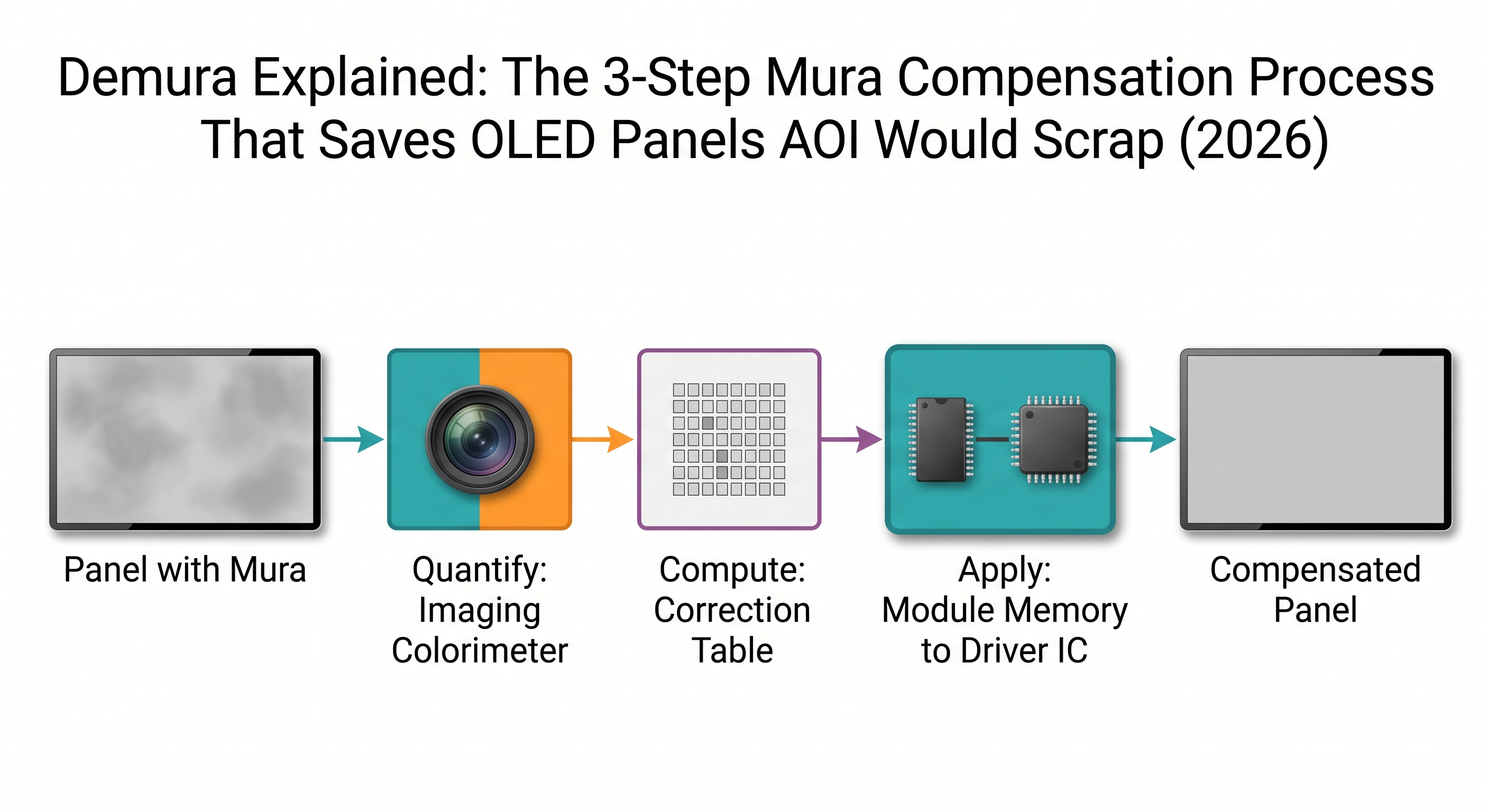
Demura is the process of measuring a display's non-uniformity pixel by pixel and then storing a correction value for every sub-pixel so the driver IC cancels the defect out during normal operation. Mura is the defect — the faint cloudy patches, bands, or blotches of uneven luminance that show up on a flat gray field. Demura is the correction, and it is not inspection: automated optical inspection (AOI) decides whether a panel passes or fails, while demura takes panels that would have failed a uniformity spec and makes them pass by rewriting the grayscale values they receive. That distinction — detect-and-reject versus measure-and-compensate — is the whole reason demura exists as a separate production step with its own metrology station, its own data pipeline, and its own line item in the module bill of materials.
By The Whitepaper Skeptic — display-panel project work plus machine-vision sub-pixel registration experience
Quick Facts
| Question | Answer |
|---|---|
| What is demura? | A per-sub-pixel compensation process: measure luminance/chromaticity non-uniformity, compute correction factors, and apply them through the display driver IC so the defect becomes invisible |
| Mura vs. demura | Mura is the visual defect (uneven luminance/color); demura is the correction applied to hide it. Searchers use the terms interchangeably, but they are opposites |
| How is it different from AOI? | AOI detects and classifies defects to sort panels; demura measures a panel that already failed uniformity spec and compensates for it electronically instead of scrapping it |
| Where is the correction data stored? | In non-volatile memory on the module (flash/OTP/EEPROM), loaded into the driver IC's demura RAM at power-on and applied to grayscale data before the source driver |
| Why is compression such a big deal? | Correction-table size sets the required non-volatile memory capacity per module, which is a real per-unit cost — hence the volume of 2025–2026 SID research on demura data compression rather than optics |
Mura vs. Demura: The Defect and the Fix Are Not the Same Word
Mura (ムラ, "unevenness") is the industry's catch-all for distributed luminance or chromaticity non-uniformity that a viewer perceives as cloudiness, banding, blotching, or a visible mura pattern on a uniform gray field. It is not a point defect. A dead pixel, a bright dot, or a line defect caused by a shorted signal trace is a discrete failure at a known coordinate; mura is a low-contrast gradient spread across a region, often too subtle to trip a rule-based inspection threshold but immediately obvious to a human eye on a mid-gray test pattern.
That difference in physical character is why the fix is different too. You can zap a shorted trace with a laser. You cannot zap a cloud. Demura instead accepts that the panel's physical response is non-uniform and corrects the input signal to compensate: if a region of sub-pixels emits 3% dimmer than the target at a given gray level, the driver sends that region a proportionally higher drive value so the output lands on target. Nothing about the panel changes. What changes is the number arriving at the source driver.
Our machine-vision defect inspection explainer covers the detection half of this — how AOI and deep-learning classifiers find defects in the first place. This piece covers what happens after a panel has been found defective and the fab has to decide what to do about it.
Repair, Demura, or Scrap: The Three Branches After a Uniformity Failure
Most explanations of display defects stop at "the panel fails inspection." In practice, a failed panel enters a three-way decision, and demura is the branch almost nobody writes about:
| Dimension | Laser repair | Demura compensation | Scrap |
|---|---|---|---|
| What it fixes | Discrete, localized defects: shorted traces, bright dots, line defects with an identifiable physical cause at a known coordinate | Distributed luminance/chromaticity non-uniformity with no single repairable cause — mura clouds, bands, gradients, per-emitter output spread | Nothing — the panel is removed from the line |
| Where in the line | Array/cell stage, at a dedicated repair station after AOI localizes the defect coordinate | Module/back-end stage, after the panel is driveable and can display test patterns | Any stage, whenever the defect is unrepairable and uncompensatable |
| What it costs | Repair-station time per defect plus laser tool capex; scales with defect count on the panel | A metrology station (imaging colorimeter) plus per-module non-volatile memory to hold the correction table — a recurring BOM cost on every unit, not just defective ones | Full accumulated value of the panel at the point of scrap |
| What it leaves behind | A physically altered panel — the defect is gone or converted to a less visible state | A physically unchanged panel plus a correction table permanently bound to that specific panel's serial identity | Nothing recoverable except materials value |
Read the middle column carefully: demura's cost is not paid per defect, it is paid per module. Once a product line adopts demura, every panel gets a metrology pass and every module carries the memory to hold its table — including panels that were fine to begin with. That is a very different economic shape from laser repair, where our panel laser repair explainer covers the per-defect, per-coordinate model. A buyer evaluating a demura station is therefore not asking "how many panels will this save?" but "what does per-module correction memory cost me across the entire production volume?"
The Three-Step Demura Workflow
The workflow that vendors and SID papers converge on has three steps, and the interesting engineering is unevenly distributed across them.
Step 1 — Quantify
A high-resolution imaging colorimeter captures the panel displaying a series of flat test patterns, and luminance and chromaticity values are extracted for every sub-pixel. This is a photometric measurement, not a pass/fail image classification: the output is a value per sub-pixel per test level, not a defect map.
Step 2 — Compute
Those measured values are compared against the target uniformity curve, and a correction factor is computed per sub-pixel — typically at several gray anchor levels, since a panel's non-uniformity is generally not constant across the full gray range.
Step 3 — Apply
The correction data is written to the module and applied at runtime by an external control IC or the display driver IC (DDIC), which modifies grayscale values before they reach the source driver.
The Data Path Under Step 3 Is Where the Cost Lives
That three-step structure is how equipment vendors describe the process in published technical material (see Sources — the Automate.org/A3 and OLED-Info mirrors of the imaging-colorimeter application paper). Break step 3 open and the economics become visible:
| Stage | What happens | Why it matters |
|---|---|---|
| Measurement | Imaging colorimeter captures per-sub-pixel luminance/chromaticity at multiple gray levels | Sets the accuracy ceiling for everything downstream; also sets station tact time |
| Correction table computation | Per-sub-pixel correction factors derived against the target uniformity curve | Determines how many gray anchor points the table must carry |
| Compression | The raw table is compressed before it is written to the module | Directly sets required flash/OTP capacity — this is the cost decision, not a footnote |
| Non-volatile storage | Compressed table written to module flash / OTP / EEPROM, bound to that specific panel | Per-module BOM line item on every unit shipped |
| Power-on load | Table decompressed and loaded into the DDIC's internal demura RAM | Constrains on-chip RAM size and boot-time budget |
| Runtime application | Correction applied to grayscale values before the source driver | Invisible to the host system — the panel simply behaves as if it were uniform |
Why Half the Research Is About Compression, Not Optics
Run the arithmetic on a 4K panel and the reason becomes obvious. A 3840 × 2160 panel has 8,294,400 pixels; with three sub-pixels each, that is 24,883,200 sub-pixel correction values per gray anchor level. Store one byte per sub-pixel and one gray level already costs roughly 24.9 MB. Carry eight gray anchor points and the uncompressed table approaches 200 MB. (That arithmetic is illustrative — it assumes a particular byte depth and anchor count to show the scaling behavior, not a vendor specification.) No one is putting 200 MB of non-volatile memory on a display module to store a correction table, which is precisely why compression is where the published research clusters.
One 2025 SID Symposium Digest paper (64-1, Xia et al.) applies a simplified H.264/AVC codec to AMOLED demura compensation data and reports better than 16:1 compression. Treat that as one team's result on their own data, not as a typical industry figure. The patent literature makes the same argument from the cost side: US20180191371A1, granted as US10224955 in 2019, covers compression and decompression of the demura table explicitly as a method for reducing required storage, and US12008954, granted in June 2024, covers compressing demura compensation values — a line of prior art running from the mid-2010s to the present whose entire premise is that table size, not measurement accuracy, is the binding constraint.
The 2025–2026 conference record points the same direction. Volume 56 of the SID Symposium Digest carried a deep-learning LCD demura algorithm from Xiao et al. (6-3, with a poster version as P-40) that trains a U-shaped network against conventional-method compensation values as labels, so a single gray-level capture stands in for the seven the conventional flow needs — a tact-time result, not an accuracy one. The same volume carried Heo et al. (28-3) on frequency-decomposition demura processing, which reports 65.6% less memory for compensation-data storage than the conventional method and states the priority in its title. Display Week 2026, held May 3–8, 2026 at the Los Angeles Convention Center, ran in the same groove: its symposium program includes work on sharing compensation memory between demura and burn-in compensation blocks and on DCT-based compression of mura data, rather than on measurement optics.
Sub-Pixel Registration: Why the Camera Became the Hard Part
There is an assumption buried in step 1 that quietly breaks at high pixel density: that a camera pixel maps cleanly onto a display sub-pixel. It does not, and it stopped doing so as soon as emissive panel PPI outran imaging-colorimeter sensor resolution. When multiple display sub-pixels fall inside one camera pixel's footprint — or worse, when a sub-pixel straddles a camera pixel boundary — the measured value is a blend, and correcting from a blended measurement smears the correction across neighbors instead of fixing the sub-pixel that was actually off.
This is the same registration problem I dealt with on the perception side of autonomous mobile robot work: when a sensor grid and a target grid are not aligned at integer offsets, you either resample with sub-pixel interpolation or you accept systematic bias. Metrology vendors solved it the same way. Radiant Vision Systems' Fractional Pixel Method, published as SID Digest 71-1 (Pedeville et al.) back in 2020, defines sub-pixel regions of interest with fractional sensor-pixel boundaries so the measurement recovers accuracy when the camera's native resolution is insufficient. TechnoTeam's LMK DeMURA product line carries an Advanced Pixel Registration (APR) capability for the same reason, assigning measured luminance to the correct pixel index from a single capture instead of requiring neighboring pixels to be switched off. Neither of those features would exist if a camera pixel still mapped one-to-one onto a display sub-pixel.
This is also why demura is now unavoidable in the highest-density emissive categories. Our OLEDoS microdisplay explainer covers panels in the thousands-of-PPI range, where a conventional colorimeter's per-pixel mapping assumption is simply gone. And micro-LED mass transfer produces panels assembled from millions of individually transferred dies, each with its own forward-voltage and luminous-efficiency spread — a per-emitter output distribution that is inherent to the assembly method rather than a process excursion. A panel like that cannot ship without per-pixel correction, because there is no "uniform" state to manufacture toward in the first place.
The Real Production Constraint Is Tact Time, Not Accuracy
The specification a demura station gets evaluated on is usually measurement accuracy. The thing that actually determines whether it can sit on a line is how long it holds the panel.
Every additional gray anchor level means another set of captures. Every capture means camera integration time, and for low-luminance patterns — exactly where mura is most visible — integration time is long. Add pattern-switching settling, panel handling, and the compute time to derive and compress the table, and the per-panel cycle can easily exceed the takt of the line it is supposed to feed. On the display-panel project I worked on with a global materials supplier, the recurring argument in optical inspection was never "can we measure this more precisely" — the measurement physics were understood. It was "can we measure it inside the window the line gives us," and the answer routinely forced a reduction in sampled gray levels or measurement points, with the accuracy loss absorbed by smarter interpolation rather than by more captures.
That is the practical reason interpolation-heavy and frequency-domain demura methods keep appearing in the literature: they let a station measure fewer points and reconstruct the rest, which buys back tact time. It is also why a buyer comparing demura stations should ask for cycle time at the specific gray-level count and panel size they actually run, not the vendor's headline accuracy figure. Vendor-tier differences on this kind of inspection tooling are covered in our display inspection AI vendor comparison — the same evaluation logic applies when the station's job is measurement for correction rather than pass/fail sorting.
FAQ
Q: What is the difference between mura and demura? A: Mura is the defect — distributed luminance or chromaticity non-uniformity that looks like cloudiness, banding, or blotches on a flat gray field. Demura is the correction process that measures that non-uniformity per sub-pixel and stores compensation values so the driver IC cancels it out during normal operation. The panel is not physically changed by demura; only the grayscale values it receives are.
Q: What is the difference between demura and AOI defect inspection? A: AOI detects and classifies defects to decide whether a panel passes, gets repaired, or gets scrapped. Demura assumes the defect exists and cannot be physically fixed, then compensates for it electronically. AOI is detect-and-reject; demura is measure-and-compensate. They run at different stages, use different equipment, and produce different outputs — a defect map versus a per-sub-pixel correction table.
Q: Where is demura compensation data stored? A: In non-volatile memory on the display module — flash, OTP, or EEPROM depending on the design. At power-on the data is loaded into the display driver IC's internal demura RAM and applied to grayscale values before they reach the source driver. Because the table is bound to the specific panel it was measured from, it travels with that module for the life of the product.
Q: Why does microLED need demura? A: A microLED panel is assembled from millions of individually transferred emitters, each with its own forward-voltage and efficiency variation. That per-die spread is inherent to mass transfer rather than a process fault, so there is no uniform baseline to manufacture toward — per-pixel correction is the mechanism that turns a population of slightly different emitters into a visually uniform display.
Q: Why does demura data need compression? A: Because the raw correction table scales with sub-pixel count times gray anchor levels, and it has to fit in non-volatile memory on every module. On a 4K panel that is roughly 24.9 million sub-pixel values per gray level before any compression. Table size therefore sets required flash capacity, which is a recurring per-unit BOM cost — which is why much of the recent published demura research targets compression rather than measurement optics.
Sources
- SID Display Week 2026 Symposium Program — 2026 demura memory-sharing and mura-data-compression papers; Display Week 2026 program schedule for dates and venue (May 3–8, 2026, Los Angeles Convention Center)
- SID Symposium Digest 71-1, Pedeville, Rouse and Kreysar, "Fractional Pixel Method for Improved Pixel-Level Measurement and Correction (Demura) of High-Resolution Displays," 2020, vol. 51, pp. 1056–1059
- Automate.org / A3, "Using Imaging Colorimeters to Correct OLED, MicroLED, and Other Emissive Displays for Improved Production Efficiency and Yields" — three-step demura workflow (vendor technical paper authored by Radiant Vision Systems)
- OLED-Info, "Correcting OLED and MicroLED Display Quality to Improve Production Efficiency and Yields" — mirror of the same Radiant-authored paper; states the three steps as measurement, calculation of correction factors, and application via an external control IC
- TechnoTeam, LMK DeMURA — Advanced Pixel Registration
- US20180191371A1 / US10224955, "Data compression and decompression method of demura table, and mura compensation method" — primary source for the flash-capacity/cost argument
- US12008954, "Method and system for compressing Demura compensation value" — current-art compression citation
- SID Symposium Digest 6-3 / P-40, Xiao et al., "A Novel LCD De-Mura Algorithm Based on Deep Learning," 2025, vol. 56 — U-net trained on conventional compensation values; captures reduced from seven to one
- SID Symposium Digest 28-3, Heo et al., "Frequency Decomposition-Based High-Performance Demura Processing with Low Memory Cost," 2025, vol. 56, pp. 366–368 — 65.6% compensation-data memory reduction
- SID Symposium Digest 64-1, Xia et al., "A Customized H.264/AVC Codec for AMOLED Demura Compensation Data Compression," 2025, vol. 56, pp. 546–551 — source of the >16:1 compression figure
Author Bio
This article frames demura as a data and tact-time problem rather than an optics story, and that framing is inherited rather than invented. It comes partly from display-panel project work The Whitepaper Skeptic did with a global materials supplier, and partly from years of autonomous mobile robot perception work built on the same sub-pixel registration and imaging math that demura metrology depends on. Both pointed at the same economics — the camera is rarely the expensive part, whereas the correction table you store, compress, and read back at every power-on is, and the time a station is allowed to hold a panel sets how much of that table you can afford to build.
Related Posts
- How Are OLED and LCD Displays Manufactured? A Guide to Panel Fabrication and Inspection — the pillar guide covering the full panel fabrication and inspection sequence this compensation step sits at the back end of
- Display Panel Laser Repair Explained: How Fabs Fix 3 Defect Types Without Scrapping the Panel — cluster-mate: the physical-repair branch of the same three-way decision, priced per defect rather than per module
- Machine Vision for Display Defect Inspection: How AOI and Deep Learning Catch Sub-Pixel Defects — cluster-mate: the detection step that decides which panels reach the demura branch in the first place
- Micro-LED Mass Transfer Explained: Why the Industry Needs "Six Nines" Yield to Beat OLED — cluster-mate: why per-die luminance spread after mass transfer makes per-pixel correction mandatory rather than optional
Tags
demura process, mura compensation, OLED uniformity correction, imaging colorimeter, demura data compression


Comments
Post a Comment